• 文献检索
  • 文档翻译
  • 深度研究
  • 学术资讯
  • Suppr Zotero 插件Zotero 插件
  • 邀请有礼
  • 套餐&价格
  • 历史记录
应用&插件
Suppr Zotero 插件Zotero 插件浏览器插件Mac 客户端Windows 客户端微信小程序
定价
高级版会员购买积分包购买API积分包
服务
文献检索文档翻译深度研究API 文档MCP 服务
关于我们
关于 Suppr公司介绍联系我们用户协议隐私条款
关注我们

Suppr 超能文献

核心技术专利:CN118964589B侵权必究
粤ICP备2023148730 号-1Suppr @ 2026

文献检索

告别复杂PubMed语法,用中文像聊天一样搜索,搜遍4000万医学文献。AI智能推荐,让科研检索更轻松。

立即免费搜索

文件翻译

保留排版,准确专业,支持PDF/Word/PPT等文件格式,支持 12+语言互译。

免费翻译文档

深度研究

AI帮你快速写综述,25分钟生成高质量综述,智能提取关键信息,辅助科研写作。

立即免费体验

高压气相外延法生长 GaN 晶体中的应力对 MOCVD-GaN/6H-SiC 衬底的影响。

Influence of stress in GaN crystals grown by HVPE on MOCVD-GaN/6H-SiC substrate.

机构信息

State Key Lab of Crystal Materials, Shandong University, Jinan, 250100, P.R. China.

Department of Materials Science and Engineering, Qilu University of Technology, Jinan 250353, P. R. China.

出版信息

Sci Rep. 2014 Feb 26;4:4179. doi: 10.1038/srep04179.

DOI:10.1038/srep04179
PMID:24569601
原文链接:https://pmc.ncbi.nlm.nih.gov/articles/PMC3935196/
Abstract

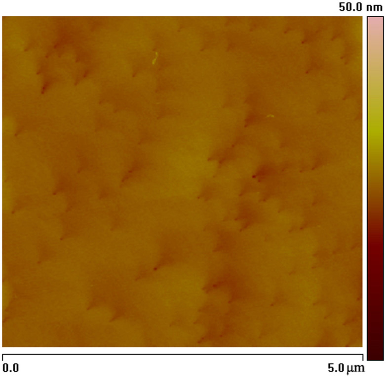
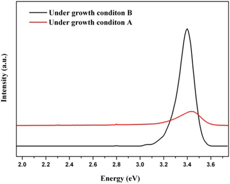
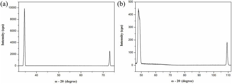
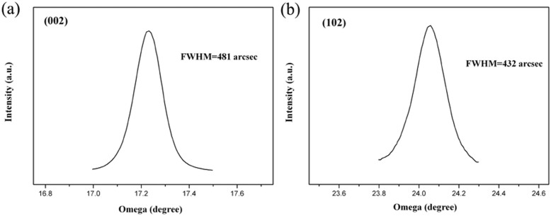
GaN crystals without cracks were successfully grown on a MOCVD-GaN/6H-SiC (MGS) substrate with a low V/III ratio of 20 at initial growth. With a high V/III ratio of 80 at initial growth, opaque GaN polycrystals were obtained. The structural analysis and optical characterization reveal that stress has a great influence on the growth of the epitaxial films. An atomic level model is used to explain these phenomena during crystal growth. It is found that atomic mobility is retarded by compressive stress and enhanced by tensile stress.

摘要

成功地在初始生长时 V/III 比为 20 的低 GaN/MOCVD-GaN/6H-SiC (MGS) 衬底上生长出无裂纹 GaN 晶体。而在初始生长时 V/III 比为 80 时,则得到不透明的 GaN 多晶。结构分析和光学特性表明,在薄膜生长过程中,应变速率对其生长有很大的影响。利用原子级模型来解释这些在晶体生长过程中的现象。结果表明,压应力会阻碍原子迁移,而张应力则会增强原子迁移。

https://cdn.ncbi.nlm.nih.gov/pmc/blobs/bc92/3935196/7f6024cadf11/srep04179-f8.jpg
https://cdn.ncbi.nlm.nih.gov/pmc/blobs/bc92/3935196/e372a4963af8/srep04179-f1.jpg
https://cdn.ncbi.nlm.nih.gov/pmc/blobs/bc92/3935196/75539bccdf0d/srep04179-f2.jpg
https://cdn.ncbi.nlm.nih.gov/pmc/blobs/bc92/3935196/2c9b97fb0158/srep04179-f3.jpg
https://cdn.ncbi.nlm.nih.gov/pmc/blobs/bc92/3935196/5fe420db659a/srep04179-f4.jpg
https://cdn.ncbi.nlm.nih.gov/pmc/blobs/bc92/3935196/999707739c15/srep04179-f5.jpg
https://cdn.ncbi.nlm.nih.gov/pmc/blobs/bc92/3935196/b98deeab185d/srep04179-f6.jpg
https://cdn.ncbi.nlm.nih.gov/pmc/blobs/bc92/3935196/bcfb66ff09dd/srep04179-f7.jpg
https://cdn.ncbi.nlm.nih.gov/pmc/blobs/bc92/3935196/7f6024cadf11/srep04179-f8.jpg

相似文献

1
Influence of stress in GaN crystals grown by HVPE on MOCVD-GaN/6H-SiC substrate.高压气相外延法生长 GaN 晶体中的应力对 MOCVD-GaN/6H-SiC 衬底的影响。
Sci Rep. 2014 Feb 26;4:4179. doi: 10.1038/srep04179.
2
The investigation of stress in freestanding GaN crystals grown from Si substrates by HVPE.采用 HVPE 法在 Si 衬底上生长的 GaN 自支撑晶体中的应力研究。
Sci Rep. 2017 Aug 17;7(1):8587. doi: 10.1038/s41598-017-08905-y.
3
Direct growth of freestanding GaN on C-face SiC by HVPE.通过氢化物气相外延法在C面碳化硅上直接生长独立的氮化镓。
Sci Rep. 2015 Jun 2;5:10748. doi: 10.1038/srep10748.
4
Investigation of cracks in GaN films grown by combined hydride and metal organic vapor-phase epitaxial method.通过氢化物与金属有机气相外延相结合的方法生长的氮化镓薄膜中的裂纹研究。
Nanoscale Res Lett. 2011 Jan 12;6(1):69. doi: 10.1186/1556-276X-6-69.
5
Microstructural Characterization of GaN Grown on SiC.在碳化硅上生长的氮化镓的微观结构表征
Microsc Microanal. 2019 Dec;25(6):1383-1393. doi: 10.1017/S1431927619014739.
6
High quality self-separated GaN crystal grown on a novel nanoporous template by HVPE.通过氢化物气相外延法在新型纳米多孔模板上生长的高质量自分离氮化镓晶体。
Sci Rep. 2018 Feb 16;8(1):3166. doi: 10.1038/s41598-018-21607-3.
7
Electronic states of deep trap levels in a-plane GaN templates grown on r-plane sapphire by HVPE.通过氢化物气相外延(HVPE)在r面蓝宝石上生长的a面氮化镓模板中深陷阱能级的电子态。
Sci Rep. 2018 May 18;8(1):7814. doi: 10.1038/s41598-018-26290-y.
8
An aberration-corrected STEM study of structural defects in epitaxial GaN thin films grown by ion beam assisted MBE.离子束辅助分子束外延生长的外延氮化镓薄膜结构缺陷的像差校正扫描透射电子显微镜研究。
Micron. 2015 Jun;73:1-8. doi: 10.1016/j.micron.2015.03.006. Epub 2015 Mar 23.
9
Fabrication of 2-Inch Free-Standing GaN Substrate on Sapphire With a Combined Buffer Layer by HVPE.通过氢化物气相外延法在蓝宝石上制备具有复合缓冲层的2英寸自支撑氮化镓衬底。
Front Chem. 2021 Apr 22;9:671720. doi: 10.3389/fchem.2021.671720. eCollection 2021.
10
High Thermal Dissipation of Normally off p-GaN Gate AlGaN/GaN HEMTs on 6-Inch N-Doped Low-Resistivity SiC Substrate.6英寸N型低电阻率碳化硅衬底上常关型p-GaN栅极AlGaN/GaN高电子迁移率晶体管的高热耗散
Micromachines (Basel). 2021 May 1;12(5):509. doi: 10.3390/mi12050509.

引用本文的文献

1
Fabrication of gallium nitride and nitrogen doped single layer graphene hybrid heterostructures for high performance photodetectors.用于高性能光电探测器的氮化镓与氮掺杂单层石墨烯混合异质结构的制备
Sci Rep. 2020 Sep 2;10(1):14507. doi: 10.1038/s41598-020-71514-9.
2
Direct Observation of the Biaxial Stress Effect on Efficiency Droop in GaN-based Light-emitting Diode under Electrical Injection.电注入下基于氮化镓的发光二极管中双轴应力对效率下降影响的直接观测
Sci Rep. 2015 Dec 4;5:17227. doi: 10.1038/srep17227.
3
Three-dimensional Aerographite-GaN hybrid networks: single step fabrication of porous and mechanically flexible materials for multifunctional applications.

本文引用的文献

1
Strain effects on excitonic transitions in GaN: Deformation potentials.
Phys Rev B Condens Matter. 1996 Nov 15;54(19):13460-13463. doi: 10.1103/physrevb.54.13460.
2
Atomistic Processes in the Early Stages of Thin-Film Growth.薄膜生长早期阶段的原子过程。
Science. 1997 Apr 18;276(5311):377-83. doi: 10.1126/science.276.5311.377.
三维气凝胶石墨-氮化镓混合网络:用于多功能应用的多孔且机械柔性材料的一步法制备
Sci Rep. 2015 Mar 6;5:8839. doi: 10.1038/srep08839.