• 文献检索
  • 文档翻译
  • 深度研究
  • 学术资讯
  • Suppr Zotero 插件Zotero 插件
  • 邀请有礼
  • 套餐&价格
  • 历史记录
应用&插件
Suppr Zotero 插件Zotero 插件浏览器插件Mac 客户端Windows 客户端微信小程序
定价
高级版会员购买积分包购买API积分包
服务
文献检索文档翻译深度研究API 文档MCP 服务
关于我们
关于 Suppr公司介绍联系我们用户协议隐私条款
关注我们

Suppr 超能文献

核心技术专利:CN118964589B侵权必究
粤ICP备2023148730 号-1Suppr @ 2026

文献检索

告别复杂PubMed语法,用中文像聊天一样搜索,搜遍4000万医学文献。AI智能推荐,让科研检索更轻松。

立即免费搜索

文件翻译

保留排版,准确专业,支持PDF/Word/PPT等文件格式,支持 12+语言互译。

免费翻译文档

深度研究

AI帮你快速写综述,25分钟生成高质量综述,智能提取关键信息,辅助科研写作。

立即免费体验

采用 HVPE 法在 Si 衬底上生长的 GaN 自支撑晶体中的应力研究。

The investigation of stress in freestanding GaN crystals grown from Si substrates by HVPE.

机构信息

Korea Basic Science Institute, Daejeon, 169-148, Republic of Korea.

Ecole Polytechnique Fédérale de Lausanne, Laboratory of Semiconductor Materials, Lausanne, 1015, Switzerland.

出版信息

Sci Rep. 2017 Aug 17;7(1):8587. doi: 10.1038/s41598-017-08905-y.

DOI:10.1038/s41598-017-08905-y
PMID:28819151
原文链接:https://pmc.ncbi.nlm.nih.gov/articles/PMC5561118/
Abstract

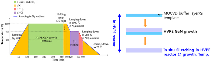
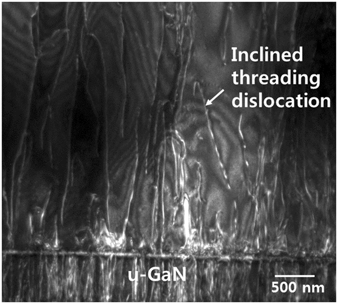
We investigate the stress evolution of 400 µm-thick freestanding GaN crystals grown from Si substrates by hydride vapour phase epitaxy (HVPE) and the in situ removal of Si substrates. The stress generated in growing GaN can be tuned by varying the thickness of the MOCVD AlGaN/AlN buffer layers. Micro Raman analysis shows the presence of slight tensile stress in the freestanding GaN crystals and no stress accumulation in HVPE GaN layers during the growth. Additionally, it is demonstrated that the residual tensile stress in HVPE GaN is caused only by elastic stress arising from the crystal quality difference between Ga- and N-face GaN. TEM analysis revealed that the dislocations in freestanding GaN crystals have high inclination angles that are attributed to the stress relaxation of the crystals. We believe that the understanding and characterization on the structural properties of the freestanding GaN crystals will help us to use these crystals for high-performance opto-electronic devices.

摘要

我们研究了通过氢化物气相外延(HVPE)和 Si 衬底的原位去除生长的 400μm 厚的自由 standing GaN 晶体的应力演变。通过改变 MOCVD AlGaN/AlN 缓冲层的厚度,可以调整生长 GaN 时产生的应力。微拉曼分析表明,自由 standing GaN 晶体中存在轻微的拉伸应力,并且在 HVPE GaN 层的生长过程中没有应力积累。此外,证明 HVPE GaN 中的残余拉伸应力仅由 GaN 和 N 面 GaN 之间的晶体质量差异引起的弹性应力引起。TEM 分析表明,自由 standing GaN 晶体中的位错具有较高的倾斜角,这归因于晶体的应力松弛。我们相信,对自由 standing GaN 晶体的结构特性的理解和表征将有助于我们将这些晶体用于高性能光电设备。

https://cdn.ncbi.nlm.nih.gov/pmc/blobs/8e47/5561118/2efff214e74d/41598_2017_8905_Fig4_HTML.jpg
https://cdn.ncbi.nlm.nih.gov/pmc/blobs/8e47/5561118/77efe43734f8/41598_2017_8905_Fig1_HTML.jpg
https://cdn.ncbi.nlm.nih.gov/pmc/blobs/8e47/5561118/29c086e9356a/41598_2017_8905_Fig2_HTML.jpg
https://cdn.ncbi.nlm.nih.gov/pmc/blobs/8e47/5561118/74521c9bf208/41598_2017_8905_Fig3_HTML.jpg
https://cdn.ncbi.nlm.nih.gov/pmc/blobs/8e47/5561118/2efff214e74d/41598_2017_8905_Fig4_HTML.jpg

相似文献

1
The investigation of stress in freestanding GaN crystals grown from Si substrates by HVPE.采用 HVPE 法在 Si 衬底上生长的 GaN 自支撑晶体中的应力研究。
Sci Rep. 2017 Aug 17;7(1):8587. doi: 10.1038/s41598-017-08905-y.
2
The investigation of removal of Si substrates for freestanding GaN crystals by HVPE.通过氢化物气相外延法去除用于独立氮化镓晶体的硅衬底的研究。
RSC Adv. 2018 Mar 29;8(22):12310-12314. doi: 10.1039/c8ra01347k. eCollection 2018 Mar 26.
3
Electronic states of deep trap levels in a-plane GaN templates grown on r-plane sapphire by HVPE.通过氢化物气相外延(HVPE)在r面蓝宝石上生长的a面氮化镓模板中深陷阱能级的电子态。
Sci Rep. 2018 May 18;8(1):7814. doi: 10.1038/s41598-018-26290-y.
4
Direct growth of freestanding GaN on C-face SiC by HVPE.通过氢化物气相外延法在C面碳化硅上直接生长独立的氮化镓。
Sci Rep. 2015 Jun 2;5:10748. doi: 10.1038/srep10748.
5
First observation of electronic trap levels in freestanding GaN crystals extracted from Si substrates by hydride vapour phase epitaxy.首次观察到通过氢化物气相外延从硅衬底上提取的独立式氮化镓晶体中的电子陷阱能级。
Sci Rep. 2019 May 9;9(1):7128. doi: 10.1038/s41598-019-43583-y.
6
High quality self-separated GaN crystal grown on a novel nanoporous template by HVPE.通过氢化物气相外延法在新型纳米多孔模板上生长的高质量自分离氮化镓晶体。
Sci Rep. 2018 Feb 16;8(1):3166. doi: 10.1038/s41598-018-21607-3.
7
Fabrication of 2-Inch Free-Standing GaN Substrate on Sapphire With a Combined Buffer Layer by HVPE.通过氢化物气相外延法在蓝宝石上制备具有复合缓冲层的2英寸自支撑氮化镓衬底。
Front Chem. 2021 Apr 22;9:671720. doi: 10.3389/fchem.2021.671720. eCollection 2021.
8
Coordinated stress management and dislocation control in GaN growth on Si (111) substrates by using a carbon nanotube mask.采用碳纳米管掩模在 Si(111)衬底上协调 GaN 生长的应变速率管理和位错控制。
Nanoscale. 2019 Mar 7;11(10):4489-4495. doi: 10.1039/c8nr10289a.
9
Gradual tilting of crystallographic orientation and configuration of dislocations in GaN selectively grown by vapour phase epitaxy methods.通过气相外延法选择性生长的GaN中晶体取向的逐渐倾斜和位错的组态
J Electron Microsc (Tokyo). 2000;49(2):331-8. doi: 10.1093/oxfordjournals.jmicro.a023813.
10
Influence of stress in GaN crystals grown by HVPE on MOCVD-GaN/6H-SiC substrate.高压气相外延法生长 GaN 晶体中的应力对 MOCVD-GaN/6H-SiC 衬底的影响。
Sci Rep. 2014 Feb 26;4:4179. doi: 10.1038/srep04179.

引用本文的文献

1
A Comprehensive Review of Group-III Nitride Light-Emitting Diodes: From Millimeter to Micro-Nanometer Scales.III族氮化物发光二极管综述:从毫米到微纳米尺度
Micromachines (Basel). 2024 Sep 25;15(10):1188. doi: 10.3390/mi15101188.
2
Stress-engineered growth of homoepitaxial GaN crystals using hydride vapor phase epitaxy.
RSC Adv. 2018 Oct 17;8(62):35571-35574. doi: 10.1039/c8ra06438e. eCollection 2018 Oct 15.
3
The investigation of removal of Si substrates for freestanding GaN crystals by HVPE.通过氢化物气相外延法去除用于独立氮化镓晶体的硅衬底的研究。

本文引用的文献

1
Growth of high quality and uniformity AlGaN/GaN heterostructures on Si substrates using a single AlGaN layer with low Al composition.使用具有低铝成分的单一氮化铝镓层在硅衬底上生长高质量且均匀的氮化铝镓/氮化镓异质结构。
Sci Rep. 2016 Mar 10;6:23020. doi: 10.1038/srep23020.
2
Microstructures and growth mechanisms of GaN films epitaxially grown on AlN/Si hetero-structures by pulsed laser deposition at different temperatures.通过脉冲激光沉积在不同温度下在AlN/Si异质结构上外延生长的GaN薄膜的微观结构和生长机制。
Sci Rep. 2015 Nov 13;5:16453. doi: 10.1038/srep16453.
3
Ultralow threading dislocation density in GaN epilayer on near-strain-free GaN compliant buffer layer and its applications in hetero-epitaxial LEDs.
RSC Adv. 2018 Mar 29;8(22):12310-12314. doi: 10.1039/c8ra01347k. eCollection 2018 Mar 26.
4
Exploring an Approach toward the Intrinsic Limits of GaN Electronics.探索氮化镓电子学固有极限的方法。
ACS Appl Mater Interfaces. 2020 Mar 18;12(11):12949-12954. doi: 10.1021/acsami.9b19697. Epub 2020 Mar 5.
5
First observation of electronic trap levels in freestanding GaN crystals extracted from Si substrates by hydride vapour phase epitaxy.首次观察到通过氢化物气相外延从硅衬底上提取的独立式氮化镓晶体中的电子陷阱能级。
Sci Rep. 2019 May 9;9(1):7128. doi: 10.1038/s41598-019-43583-y.
近无应变氮化镓柔性缓冲层上氮化镓外延层中的超低 threading 位错密度及其在异质外延发光二极管中的应用
Sci Rep. 2015 Sep 2;5:13671. doi: 10.1038/srep13671.
4
Direct growth of freestanding GaN on C-face SiC by HVPE.通过氢化物气相外延法在C面碳化硅上直接生长独立的氮化镓。
Sci Rep. 2015 Jun 2;5:10748. doi: 10.1038/srep10748.
5
A GaN bulk crystal with improved structural quality grown by the ammonothermal method.通过氨热法生长的具有改善结构质量的氮化镓块状晶体。
Nat Mater. 2007 Aug;6(8):568-71. doi: 10.1038/nmat1955. Epub 2007 Jul 1.
6
Raman scattering and x-ray-absorption spectroscopy in gallium nitride under high pressure.
Phys Rev B Condens Matter. 1992 Jan 1;45(1):83-89. doi: 10.1103/physrevb.45.83.