Ji Dengxin, Song Haomin, Zeng Xie, Hu Haifeng, Liu Kai, Zhang Nan, Gan Qiaoqiang
Department of Electrical Engineering, University at Buffalo, The State University of New York, Buffalo, NY 14260.
Sci Rep. 2014 Mar 28;4:4498. doi: 10.1038/srep04498.
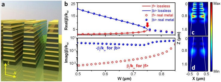
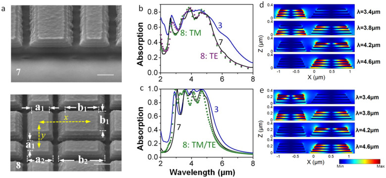
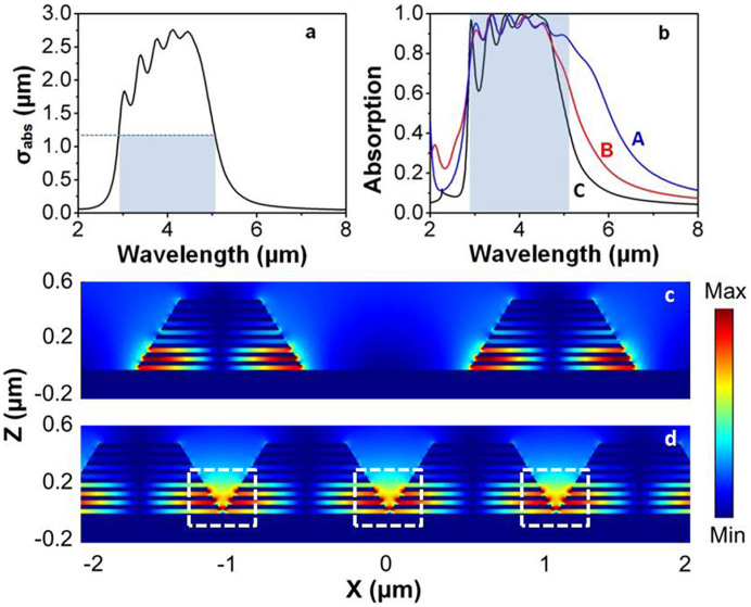
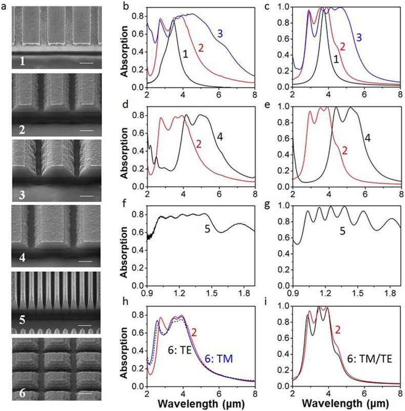
Perfect absorbers are important optical/thermal components required by a variety of applications, including photon/thermal-harvesting, thermal energy recycling, and vacuum heat liberation. While there is great interest in achieving highly absorptive materials exhibiting large broadband absorption using optically thick, micro-structured materials, it is still challenging to realize ultra-compact subwavelength absorber for on-chip optical/thermal energy applications. Here we report the experimental realization of an on-chip broadband super absorber structure based on hyperbolic metamaterial waveguide taper array with strong and tunable absorption profile from near-infrared to mid-infrared spectral region. The ability to efficiently produce broadband, highly confined and localized optical fields on a chip is expected to create new regimes of optical/thermal physics, which holds promise for impacting a broad range of energy technologies ranging from photovoltaics, to thin-film thermal absorbers/emitters, to optical-chemical energy harvesting.
完美吸收体是各种应用所需的重要光学/热学组件,包括光子/热收集、热能回收和真空热释放。虽然人们对使用光学厚度较大的微结构材料来实现具有大宽带吸收的高吸收性材料非常感兴趣,但要实现用于片上光学/热能应用的超紧凑亚波长吸收体仍然具有挑战性。在此,我们报告了一种基于双曲线超材料波导锥形阵列的片上宽带超级吸收体结构的实验实现,该结构在近红外到中红外光谱区域具有强且可调的吸收特性。在芯片上高效产生宽带、高度受限和局域化光场的能力有望开创光学/热物理学的新领域,这有望对从光伏到薄膜热吸收器/发射器再到光化学能量收集等广泛的能源技术产生影响。