• 文献检索
  • 文档翻译
  • 深度研究
  • 学术资讯
  • Suppr Zotero 插件Zotero 插件
  • 邀请有礼
  • 套餐&价格
  • 历史记录
应用&插件
Suppr Zotero 插件Zotero 插件浏览器插件Mac 客户端Windows 客户端微信小程序
定价
高级版会员购买积分包购买API积分包
服务
文献检索文档翻译深度研究API 文档MCP 服务
关于我们
关于 Suppr公司介绍联系我们用户协议隐私条款
关注我们

Suppr 超能文献

核心技术专利:CN118964589B侵权必究
粤ICP备2023148730 号-1Suppr @ 2026

文献检索

告别复杂PubMed语法,用中文像聊天一样搜索,搜遍4000万医学文献。AI智能推荐,让科研检索更轻松。

立即免费搜索

文件翻译

保留排版,准确专业,支持PDF/Word/PPT等文件格式,支持 12+语言互译。

免费翻译文档

深度研究

AI帮你快速写综述,25分钟生成高质量综述,智能提取关键信息,辅助科研写作。

立即免费体验

基于多层 WS₂ 纳米片的光响应和气体传感场效应晶体管。

Photoresponsive and gas sensing field-effect transistors based on multilayer WS₂ nanoflakes.

机构信息

State Key Laboratory for Superlattices and Microstructures, Institute of Semiconductors, Chinese Academy of SciencesP.O. Box 912, Beijing 100083, China.

Nano-Science Center & Department of Chemistry, University of Copenhagen, Universitetsparken 5, DK-2100 Copenhagen Ø, Denmark.

出版信息

Sci Rep. 2014 Jun 9;4:5209. doi: 10.1038/srep05209.

DOI:10.1038/srep05209
PMID:24909387
原文链接:https://pmc.ncbi.nlm.nih.gov/articles/PMC4048886/
Abstract

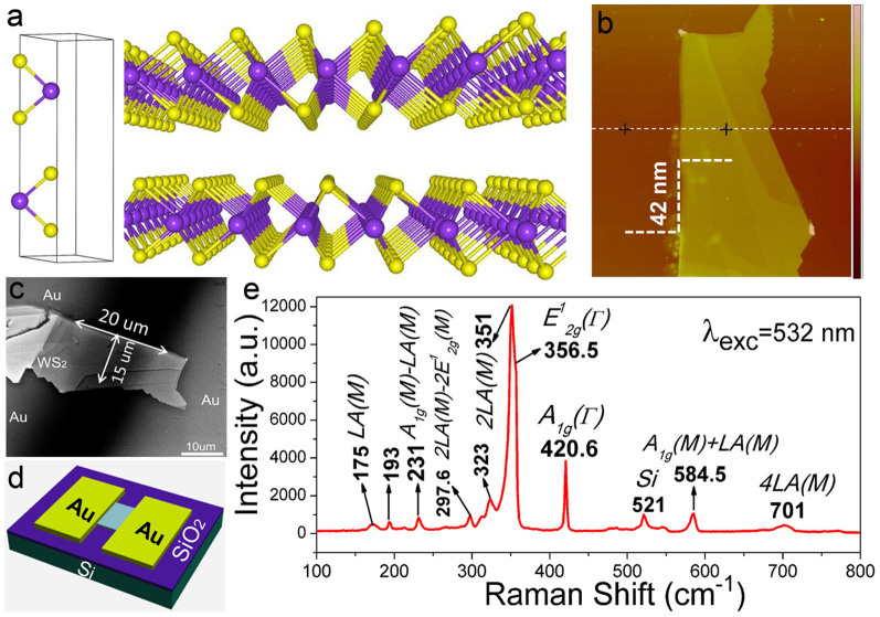
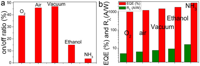
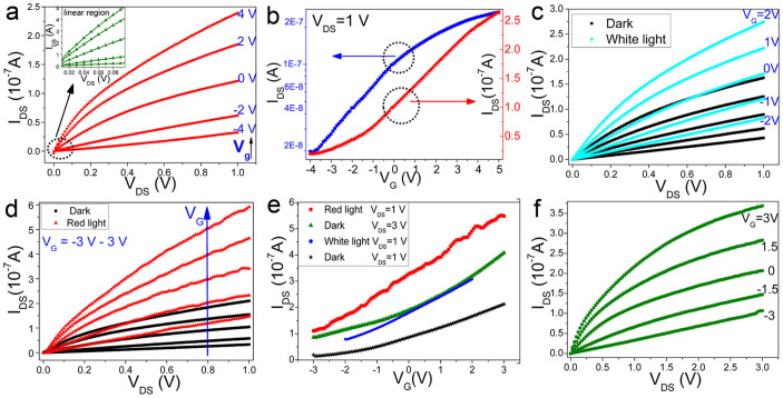
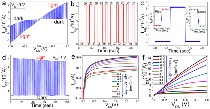
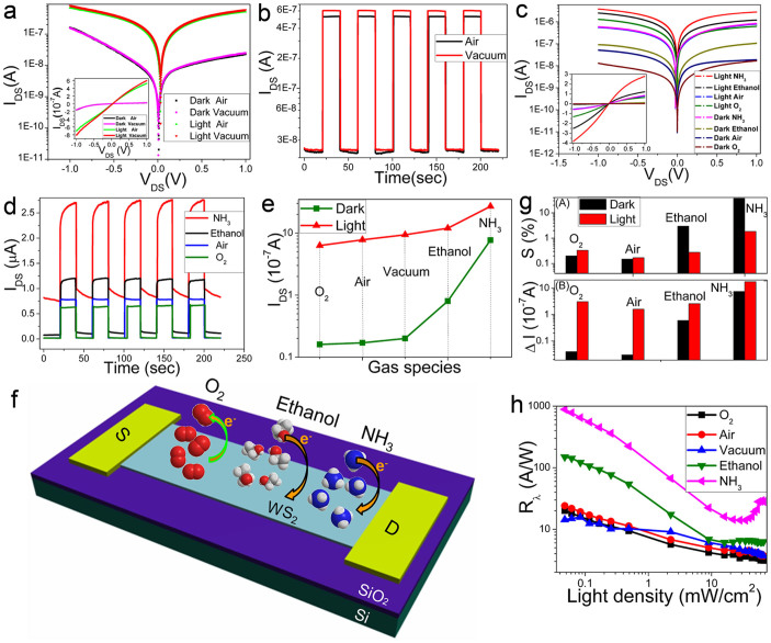
The photoelectrical properties of multilayer WS₂ nanoflakes including field-effect, photosensitive and gas sensing are comprehensively and systematically studied. The transistors perform an n-type behavior with electron mobility of 12 cm(2)/Vs and exhibit high photosensitive characteristics with response time (τ) of <20 ms, photo-responsivity (Rλ) of 5.7 A/W and external quantum efficiency (EQE) of 1118%. In addition, charge transfer can appear between the multilayer WS₂ nanoflakes and the physical-adsorbed gas molecules, greatly influencing the photoelectrical properties of our devices. The ethanol and NH₃ molecules can serve as electron donors to enhance the Rλ and EQE significantly. Under the NH3 atmosphere, the maximum Rλ and EQE can even reach 884 A/W and 1.7 × 10(5)%, respectively. This work demonstrates that multilayer WS₂ nanoflakes possess important potential for applications in field-effect transistors, highly sensitive photodetectors, and gas sensors, and it will open new way to develop two-dimensional (2D) WS₂-based optoelectronics.

摘要

我们综合系统地研究了多层 WS₂ 纳米片的光电性能,包括场效应、光敏和气体传感。晶体管表现出 n 型行为,电子迁移率为 12 cm²/Vs,并表现出高灵敏度的光敏特性,响应时间(τ)<20 ms,光响应率(Rλ)为 5.7 A/W,外量子效率(EQE)为 1118%。此外,多层 WS₂ 纳米片与物理吸附气体分子之间可以发生电荷转移,这极大地影响了我们器件的光电性能。乙醇和 NH₃ 分子可以作为电子供体,显著增强 Rλ 和 EQE。在 NH₃ 气氛下,最大的 Rλ 和 EQE 甚至可以分别达到 884 A/W 和 1.7×10(5) %。这项工作表明,多层 WS₂ 纳米片在场效应晶体管、高灵敏度光电探测器和气体传感器方面具有重要的应用潜力,为开发基于二维(2D)WS₂ 的光电技术开辟了新途径。

https://cdn.ncbi.nlm.nih.gov/pmc/blobs/55ba/4048886/2e21d6c6e232/srep05209-f5.jpg
https://cdn.ncbi.nlm.nih.gov/pmc/blobs/55ba/4048886/230c7656b1aa/srep05209-f1.jpg
https://cdn.ncbi.nlm.nih.gov/pmc/blobs/55ba/4048886/edcf02d8a0a0/srep05209-f2.jpg
https://cdn.ncbi.nlm.nih.gov/pmc/blobs/55ba/4048886/7b3a7cb73403/srep05209-f3.jpg
https://cdn.ncbi.nlm.nih.gov/pmc/blobs/55ba/4048886/bcdaf388c82a/srep05209-f4.jpg
https://cdn.ncbi.nlm.nih.gov/pmc/blobs/55ba/4048886/2e21d6c6e232/srep05209-f5.jpg

相似文献

1
Photoresponsive and gas sensing field-effect transistors based on multilayer WS₂ nanoflakes.基于多层 WS₂ 纳米片的光响应和气体传感场效应晶体管。
Sci Rep. 2014 Jun 9;4:5209. doi: 10.1038/srep05209.
2
Tunable Polarity Behavior and High-Performance Photosensitive Characteristics in Schottky-Barrier Field-Effect Transistors Based on Multilayer WS.基于多层 WS 的肖特基势垒场效应晶体管中的可调极性行为和高性能光敏特性。
ACS Appl Mater Interfaces. 2018 Jan 24;10(3):2745-2751. doi: 10.1021/acsami.7b18370. Epub 2018 Jan 8.
3
Growth of Ultraflat PbI Nanoflakes by Solvent Evaporation Suppression for High-Performance UV Photodetectors.通过抑制溶剂蒸发生长超扁平PbI纳米片用于高性能紫外光电探测器
Small. 2019 Aug;15(33):e1901767. doi: 10.1002/smll.201901767. Epub 2019 Jun 25.
4
Few-layer InPSe nanoflakes for high detectivity photodetectors.用于高探测率光电探测器的少层InPSe纳米片
Nanoscale. 2021 Feb 14;13(6):3757-3766. doi: 10.1039/d0nr07987a. Epub 2021 Feb 8.
5
High photosensitivity and broad spectral response of multi-layered germanium sulfide transistors.多层硫化锗晶体管的高光敏性和宽光谱响应
Nanoscale. 2016 Jan 28;8(4):2284-92. doi: 10.1039/c5nr05988g.
6
High on/off ratio photosensitive field effect transistors based on few layer SnS2.基于少层 SnS2 的高光/暗电流比光敏场效应晶体管。
Nanotechnology. 2016 Aug 26;27(34):34LT01. doi: 10.1088/0957-4484/27/34/34LT01. Epub 2016 Jul 15.
7
Multilayer Black Phosphorus Near-Infrared Photodetectors.多层黑磷近红外光探测器。
Sensors (Basel). 2018 May 23;18(6):1668. doi: 10.3390/s18061668.
8
Black phosphorus gas sensors.黑磷气体传感器。
ACS Nano. 2015 May 26;9(5):5618-24. doi: 10.1021/acsnano.5b01961. Epub 2015 May 6.
9
Enhanced ammonia sensing performance based on MXene-TiCT multilayer nanoflakes functionalized by tungsten trioxide nanoparticles.基于三氧化钨纳米颗粒功能化的MXene-TiCT多层纳米片的增强型氨传感性能。
J Colloid Interface Sci. 2021 Aug;595:6-14. doi: 10.1016/j.jcis.2021.03.115. Epub 2021 Mar 24.
10
High performance few-layer GaS photodetector and its unique photo-response in different gas environments.高性能少层硫化镓光电探测器及其在不同气体环境中的独特光响应。
Nanoscale. 2014 Mar 7;6(5):2582-7. doi: 10.1039/c3nr05965k. Epub 2014 Jan 27.

引用本文的文献

1
Two-Dimensional Phototransistors with van der Waals Superstructure Contacts for High-Performance Photosensing.具有范德华超结构接触的二维光电晶体管用于高性能光传感
ACS Appl Mater Interfaces. 2025 Jan 29;17(4):6521-6529. doi: 10.1021/acsami.4c16883. Epub 2025 Jan 13.
2
Design of stimuli-responsive transition metal dichalcogenides.刺激响应型过渡金属二硫属化物的设计
Commun Chem. 2024 Oct 26;7(1):241. doi: 10.1038/s42004-024-01322-z.
3
Reversible Tuning Electrical Properties in Ferroelectric SnS with NH Adsorption and Desorption.

本文引用的文献

1
Adsorption of gas molecules on monolayer MoS2 and effect of applied electric field.单层 MoS2 上气体分子的吸附及外加电场的影响。
Nanoscale Res Lett. 2013 Oct 17;8(1):425. doi: 10.1186/1556-276X-8-425.
2
Ultrasensitive photodetectors based on monolayer MoS2.基于单层 MoS2 的超高灵敏度光电探测器。
Nat Nanotechnol. 2013 Jul;8(7):497-501. doi: 10.1038/nnano.2013.100. Epub 2013 Jun 9.
3
Sensing behavior of atomically thin-layered MoS2 transistors.原子层状 MoS2 晶体管的传感行为。
通过NH吸附和解吸实现铁电体SnS电学性质的可逆调控
Nanomaterials (Basel). 2024 Oct 12;14(20):1638. doi: 10.3390/nano14201638.
4
Bending deformation modulation of the optoelectronic properties of molybdenum ditelluride doped with nonmetallic atoms X (X = B, C, N, O): a first-principles study.非金属原子X(X = B、C、N、O)掺杂碲化钼的光电性质的弯曲变形调制:第一性原理研究
J Mol Model. 2024 Mar 5;30(4):94. doi: 10.1007/s00894-024-05895-3.
5
Unleashing the potential of tungsten disulfide: Current trends in biosensing and nanomedicine applications.释放二硫化钨的潜力:生物传感与纳米医学应用的当前趋势。
Heliyon. 2024 Jan 11;10(2):e24427. doi: 10.1016/j.heliyon.2024.e24427. eCollection 2024 Jan 30.
6
Engineering the Electrical and Optical Properties of WS Monolayers via Defect Control.通过缺陷控制调控WS单层的电学和光学性质
Adv Sci (Weinh). 2024 Jan;11(4):e2305162. doi: 10.1002/advs.202305162. Epub 2023 Nov 27.
7
Photoconduction Properties in Tungsten Disulfide Nanostructures.二硫化钨纳米结构中的光电导特性
Nanomaterials (Basel). 2023 Jul 27;13(15):2190. doi: 10.3390/nano13152190.
8
Ultrahigh-responsivity waveguide-coupled optical power monitor for Si photonic circuits operating at near-infrared wavelengths.用于近红外波长工作的硅光子电路的超高响应度波导耦合光功率监视器。
Nat Commun. 2022 Dec 9;13(1):7443. doi: 10.1038/s41467-022-35206-4.
9
Nanostructured MoS and WS Photoresponses under Gas Stimuli.气体刺激下的纳米结构MoS和WS光响应。
Nanomaterials (Basel). 2022 Oct 13;12(20):3585. doi: 10.3390/nano12203585.
10
Addressing gain-bandwidth trade-off by a monolithically integrated photovoltaic transistor.通过单片集成光伏晶体管解决增益-带宽权衡问题。
Sci Adv. 2022 Sep 23;8(38):eabq0187. doi: 10.1126/sciadv.abq0187.
ACS Nano. 2013 Jun 25;7(6):4879-91. doi: 10.1021/nn400026u. Epub 2013 Jun 3.
4
High-gain phototransistors based on a CVD MoS₂ monolayer.基于 CVD MoS₂ 单层的高增益光电晶体管。
Adv Mater. 2013 Jul 5;25(25):3456-61. doi: 10.1002/adma.201301244. Epub 2013 May 23.
5
Controlled synthesis and transfer of large-area WS2 sheets: from single layer to few layers.WS2 片层的可控合成与转移:从单层到少数层。
ACS Nano. 2013 Jun 25;7(6):5235-42. doi: 10.1021/nn400971k. Epub 2013 May 15.
6
Broad-range modulation of light emission in two-dimensional semiconductors by molecular physisorption gating.二维半导体中通过分子物理吸附门控实现的宽范围光发射调控。
Nano Lett. 2013 Jun 12;13(6):2831-6. doi: 10.1021/nl4011172. Epub 2013 May 1.
7
Few-Layer MoS2 with high broadband Photogain and fast optical switching for use in harsh environments.用于恶劣环境的具有高光宽带光电增益和快速光开关的少层 MoS2。
ACS Nano. 2013 May 28;7(5):3905-11. doi: 10.1021/nn305301b. Epub 2013 Apr 22.
8
Role of metal contacts in designing high-performance monolayer n-type WSe2 field effect transistors.金属接触在设计高性能单层 n 型 WSe2 场效应晶体管中的作用。
Nano Lett. 2013 May 8;13(5):1983-90. doi: 10.1021/nl304777e. Epub 2013 Apr 4.
9
Synthesis and transfer of single-layer transition metal disulfides on diverse surfaces.单层过渡金属二硫化物在多种表面上的合成与转移。
Nano Lett. 2013 Apr 10;13(4):1852-7. doi: 10.1021/nl400687n. Epub 2013 Mar 29.
10
Highly responsive ultrathin GaS nanosheet photodetectors on rigid and flexible substrates.在刚性和柔性衬底上的高响应性超薄 GaS 纳米片光电探测器。
Nano Lett. 2013 Apr 10;13(4):1649-54. doi: 10.1021/nl400107k. Epub 2013 Mar 6.