Basyooni Mohamed A, Zaki Shrouk E, Alfryyan Nada, Tihtih Mohammed, Eker Yasin Ramazan, Attia Gamal F, Yılmaz Mücahit, Ateş Şule, Shaban Mohamed
Department of Nanotechnology and Advanced Materials, Graduate School of Applied and Natural Science, Selçuk University, Konya 42030, Turkey.
Department of Nanoscience and Nanoengineering, Institute of Science and Technology, University of Necmettin Erbakan, Konya 42060, Turkey.
Nanomaterials (Basel). 2022 Oct 13;12(20):3585. doi: 10.3390/nano12203585.
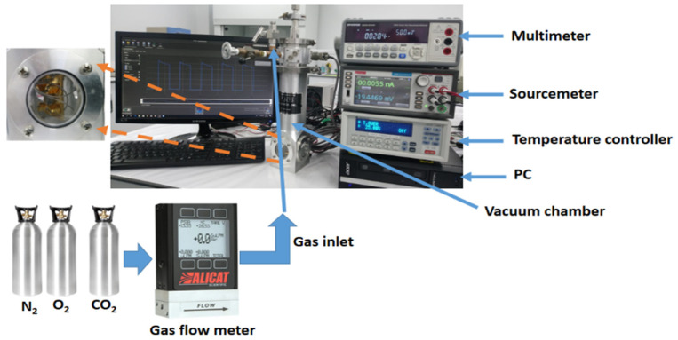
This study was on the optoelectronic properties of multilayered two-dimensional MoS and WS materials on a silicon substrate using sputtering physical vapor deposition (PVD) and chemical vapor deposition (CVD) techniques. For the first time, we report ultraviolet (UV) photoresponses under air, CO, and O environments at different flow rates. The electrical Hall effect measurement showed the existence of MoS (n-type)/Si (p-type) and WS (P-type)/Si (p-type) heterojunctions with a higher sheet carrier concentration of 5.50 × 10 cm for WS thin film. The IV electrical results revealed that WS is more reactive than MoS film under different gas stimuli. WS film showed high stability under different bias voltages, even at zero bias voltage, due to the noticeably good carrier mobility of 29.8 × 10 cm/V. WS film indicated a fast rise/decay time of 0.23/0.21 s under air while a faster response of 0.190/0.10 s under a CO environment was observed. Additionally, the external quantum efficiency of WS revealed a remarkable enhancement in the CO environment of 1.62 × 10 compared to MoS film with 6.74 × 10. According to our findings, the presence of CO on the surface of WS improves such optoelectronic properties as photocurrent gain, photoresponsivity, external quantum efficiency, and detectivity. These results indicate potential applications of WS as a photodetector under gas stimuli for future optoelectronic applications.
本研究采用溅射物理气相沉积(PVD)和化学气相沉积(CVD)技术,对硅衬底上的多层二维MoS和WS材料的光电特性进行了研究。我们首次报道了在空气、CO和O环境下不同流速下的紫外(UV)光响应。电霍尔效应测量表明存在MoS(n型)/Si(p型)和WS(P型)/Si(p型)异质结,WS薄膜的面载流子浓度较高,为5.50×10 cm 。IV电学结果表明,在不同气体刺激下,WS比MoS薄膜更具反应性。由于载流子迁移率明显良好,为29.8×10 cm/V,WS薄膜在不同偏置电压下,甚至在零偏置电压下都表现出高稳定性。WS薄膜在空气中的上升/衰减时间为0.23/0.21 s,而在CO环境下观察到更快的响应,为0.190/0.10 s。此外,WS的外量子效率在CO环境中显著提高,为1.62×10 ,而MoS薄膜为6.74×10 。根据我们的研究结果,WS表面存在CO可改善光电流增益、光响应度、外量子效率和探测率等光电特性。这些结果表明WS作为气体刺激下的光电探测器在未来光电应用中的潜在应用。