Norman Zachariah M, Anderson Nicholas C, Owen Jonathan S
Department of Chemistry, Columbia University , 3000 Broadway, MC 3121, New York, New York 10027, United States.
ACS Nano. 2014 Jul 22;8(7):7513-21. doi: 10.1021/nn502829s. Epub 2014 Jun 30.
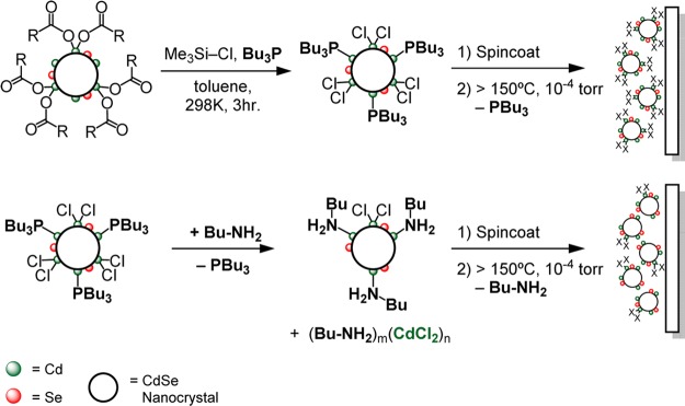
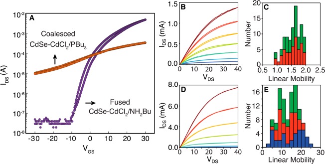
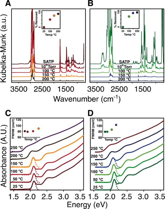
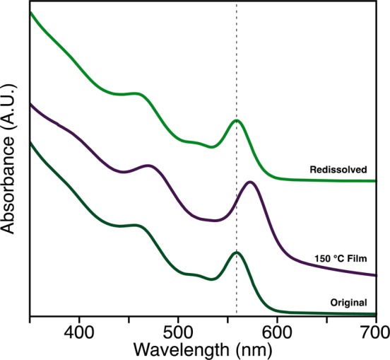
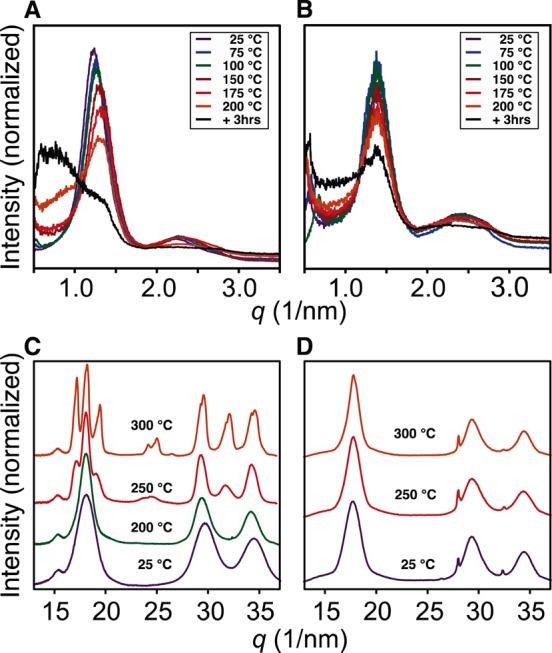
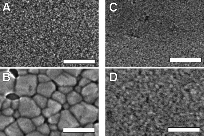
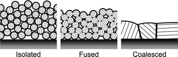
We report the evolution of electrical transport and grain size during the sintering of thin films spin-cast from soluble phosphine and amine-bound, chloride-terminated cadmium selenide nanocrystals. Sintering of the nanocrystals occurs in three distinct stages as the annealing temperature is increased: (1) reversible desorption of the organic ligands (≤150 °C), (2) irreversible particle fusion (200-300 °C), and (3) ripening of the grains to >5 nm domains (>200 °C). Grain growth occurs at 200 °C in films with 8 atom % Cl(-), while films with 3 atom % Cl(-) resist growth until 300 °C. Fused nanocrystalline thin films (grain size = 4.5-5.5 nm) on thermally grown silicon dioxide gate dielectrics produce field-effect transistors with electron mobilities as high as 25 cm(2)/(Vs) and on/off ratios of 10(5) with less than 0.5 V hysteresis in threshold voltage without the addition of indium.
我们报道了由可溶性膦和胺键合、氯封端的硒化镉纳米晶旋涂而成的薄膜在烧结过程中电输运和晶粒尺寸的演变。随着退火温度升高,纳米晶烧结发生在三个不同阶段:(1)有机配体的可逆解吸(≤150°C),(2)不可逆的颗粒融合(200 - 300°C),以及(3)晶粒长大至>5 nm 畴(>200°C)。含 8 原子% Cl⁻的薄膜在 200°C 时发生晶粒生长,而含 3 原子% Cl⁻的薄膜在 300°C 之前抑制生长。热生长二氧化硅栅介质上的熔融纳米晶薄膜(晶粒尺寸 = 4.5 - 5.5 nm)制成的场效应晶体管,电子迁移率高达 25 cm²/(Vs),开/关比为 10⁵,阈值电压滞后小于 0.5 V,且无需添加铟。