• 文献检索
  • 文档翻译
  • 深度研究
  • 学术资讯
  • Suppr Zotero 插件Zotero 插件
  • 邀请有礼
  • 套餐&价格
  • 历史记录
应用&插件
Suppr Zotero 插件Zotero 插件浏览器插件Mac 客户端Windows 客户端微信小程序
定价
高级版会员购买积分包购买API积分包
服务
文献检索文档翻译深度研究API 文档MCP 服务
关于我们
关于 Suppr公司介绍联系我们用户协议隐私条款
关注我们

Suppr 超能文献

核心技术专利:CN118964589B侵权必究
粤ICP备2023148730 号-1Suppr @ 2026

文献检索

告别复杂PubMed语法,用中文像聊天一样搜索,搜遍4000万医学文献。AI智能推荐,让科研检索更轻松。

立即免费搜索

文件翻译

保留排版,准确专业,支持PDF/Word/PPT等文件格式,支持 12+语言互译。

免费翻译文档

深度研究

AI帮你快速写综述,25分钟生成高质量综述,智能提取关键信息,辅助科研写作。

立即免费体验

利用静电俘获和渗流输运的超高灵敏度光电探测器。

Ultrasensitive photodetectors exploiting electrostatic trapping and percolation transport.

机构信息

Applied Science and Technology Graduate Program, University of California, Berkeley, California 94720, USA.

Materials Sciences Division, Lawrence Berkeley National Laboratory, 1 Cyclotron Road, Berkeley, California 94720, USA.

出版信息

Nat Commun. 2016 Jun 21;7:11924. doi: 10.1038/ncomms11924.

DOI:10.1038/ncomms11924
PMID:27323904
原文链接:https://pmc.ncbi.nlm.nih.gov/articles/PMC4919514/
Abstract

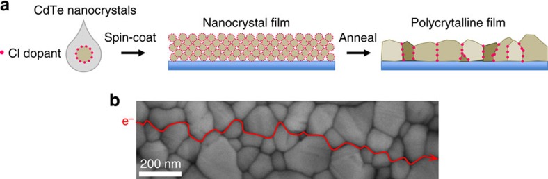
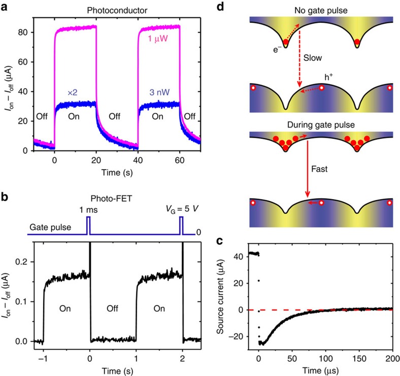
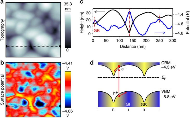
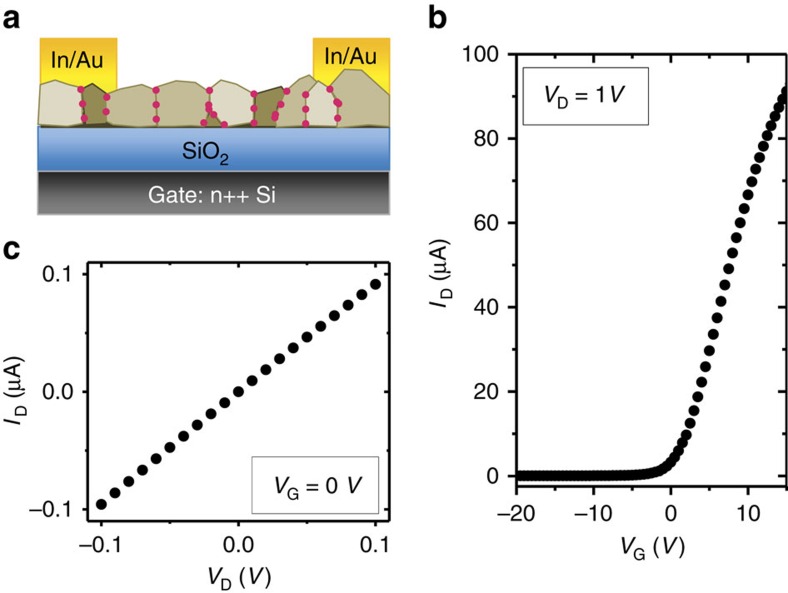
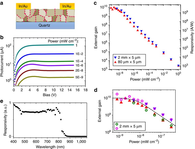
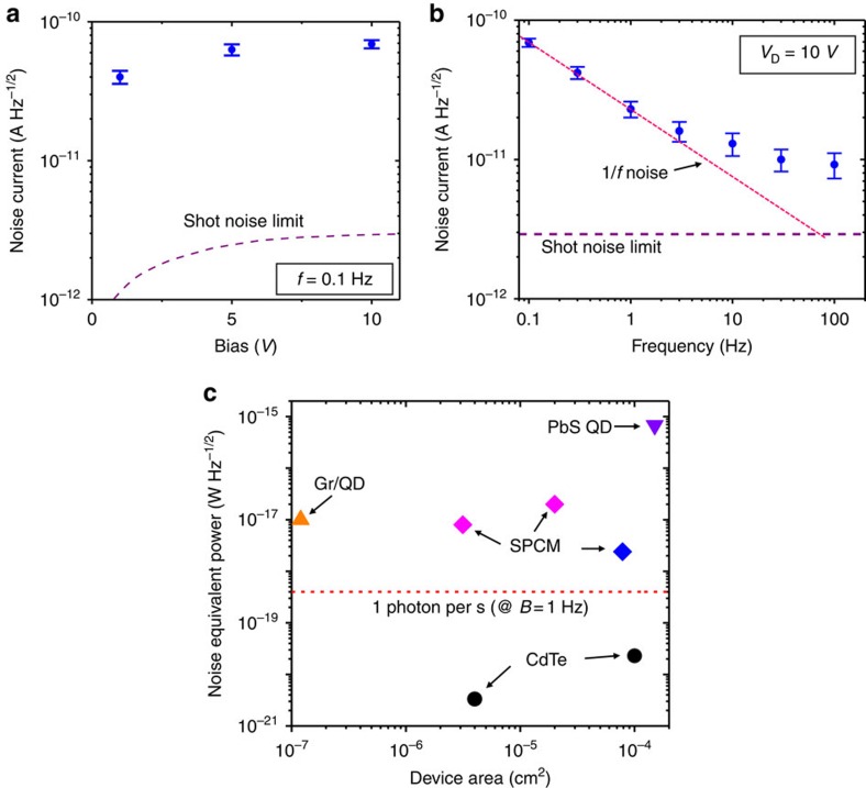
The sensitivity of semiconductor photodetectors is limited by photocarrier recombination during the carrier transport process. We developed a new photoactive material that reduces recombination by physically separating hole and electron charge carriers. This material has a specific detectivity (the ability to detect small signals) of 5 × 10(17) Jones, the highest reported in visible and infrared detectors at room temperature, and 4-5 orders of magnitude higher than that of commercial single-crystal silicon detectors. The material was fabricated by sintering chloride-capped CdTe nanocrystals into polycrystalline films, where Cl selectively segregates into grain boundaries acting as n-type dopants. Photogenerated electrons concentrate in and percolate along the grain boundaries-a network of energy valleys, while holes are confined in the grain interiors. This electrostatic field-assisted carrier separation and percolation mechanism enables an unprecedented photoconductive gain of 10(10) e(-) per photon, and allows for effective control of the device response speed by active carrier quenching.

摘要

半导体光电探测器的灵敏度受到载流子输运过程中光生载流子复合的限制。我们开发了一种新的光活性材料,通过物理分离空穴和电子电荷载流子来减少复合。这种材料的探测率(检测小信号的能力)为 5×10(17) 琼斯,在室温下的可见光和红外探测器中是报道的最高值,比商用单晶硅探测器高 4-5 个数量级。该材料是通过烧结带有氯封端的 CdTe 纳米晶制成多晶薄膜制备的,其中 Cl 选择性地在充当 n 型掺杂剂的晶界处偏析。光生电子在晶界(能量谷的网络)中浓缩并沿晶界渗滤,而空穴则局限在晶粒内部。这种静电场辅助的载流子分离和渗滤机制实现了前所未有的 10(10) 个电子/光子的光电导增益,并允许通过活性载流子猝灭来有效控制器件的响应速度。

https://cdn.ncbi.nlm.nih.gov/pmc/blobs/f127/4919514/5a7252d7fe96/ncomms11924-f6.jpg
https://cdn.ncbi.nlm.nih.gov/pmc/blobs/f127/4919514/d7e07e4aa7f5/ncomms11924-f1.jpg
https://cdn.ncbi.nlm.nih.gov/pmc/blobs/f127/4919514/19aaf917f0d8/ncomms11924-f2.jpg
https://cdn.ncbi.nlm.nih.gov/pmc/blobs/f127/4919514/c8005fd48411/ncomms11924-f3.jpg
https://cdn.ncbi.nlm.nih.gov/pmc/blobs/f127/4919514/4c61944b6b83/ncomms11924-f4.jpg
https://cdn.ncbi.nlm.nih.gov/pmc/blobs/f127/4919514/8878d5378ec4/ncomms11924-f5.jpg
https://cdn.ncbi.nlm.nih.gov/pmc/blobs/f127/4919514/5a7252d7fe96/ncomms11924-f6.jpg

相似文献

1
Ultrasensitive photodetectors exploiting electrostatic trapping and percolation transport.利用静电俘获和渗流输运的超高灵敏度光电探测器。
Nat Commun. 2016 Jun 21;7:11924. doi: 10.1038/ncomms11924.
2
High Detectivity of PbS Films Deposited on Quartz Substrates: The Role of Enhanced Photogenerated Carrier Separation.沉积在石英衬底上的硫化铅薄膜的高检测率:增强光生载流子分离的作用。
Sensors (Basel). 2023 Oct 12;23(20):8413. doi: 10.3390/s23208413.
3
Ultrasensitive solution-cast quantum dot photodetectors.超灵敏溶液浇铸量子点光电探测器。
Nature. 2006 Jul 13;442(7099):180-3. doi: 10.1038/nature04855.
4
A Novel Hybrid-Layered Organic Phototransistor Enables Efficient Intermolecular Charge Transfer and Carrier Transport for Ultrasensitive Photodetection.一种新型混合层有机光电晶体管实现了用于超灵敏光电探测的高效分子间电荷转移和载流子传输。
Adv Mater. 2019 Apr;31(16):e1900763. doi: 10.1002/adma.201900763. Epub 2019 Mar 4.
5
Noise limitations in solid state photodetectors.固态光电探测器中的噪声限制
Appl Opt. 1967 Jul 1;6(7):1145-69. doi: 10.1364/AO.6.001145.
6
Ultrafast exciton dynamics and light-driven H2 evolution in colloidal semiconductor nanorods and Pt-tipped nanorods.胶体半导体纳米棒和 Pt 尖端纳米棒中的超快激子动力学和光驱动 H2 演化。
Acc Chem Res. 2015 Mar 17;48(3):851-9. doi: 10.1021/ar500398g. Epub 2015 Feb 16.
7
Transparent and Highly Responsive Phototransistors Based on a Solution-Processed, Nanometers-Thick Active Layer, Embedding a High-Mobility Electron-Transporting Polymer and a Hole-Trapping Molecule.基于嵌入了高迁移率电子传输聚合物和空穴俘获分子的纳米厚活性层的透明且高响应性光晶体管,该活性层由溶液处理而成。
ACS Appl Mater Interfaces. 2017 Aug 30;9(34):28785-28794. doi: 10.1021/acsami.7b05259. Epub 2017 Aug 18.
8
Unveiling Defect-Mediated Charge-Carrier Recombination at the Nanometer Scale in Polycrystalline Solar Cells.揭示多晶太阳能电池中纳米尺度缺陷介导的电荷载流子复合。
ACS Appl Mater Interfaces. 2019 Dec 18;11(50):47037-47046. doi: 10.1021/acsami.9b14730. Epub 2019 Dec 4.
9
Universal Strategy To Reduce Noise Current for Sensitive Organic Photodetectors.通用策略降低敏感有机光电探测器的噪声电流。
ACS Appl Mater Interfaces. 2017 Mar 15;9(10):9176-9183. doi: 10.1021/acsami.6b16788. Epub 2017 Mar 1.
10
Achieving high sensitivity in hybrid photodetectors based on an organic single crystal and an inorganic nanocrystal array.实现基于有机单晶和无机纳米晶阵列的混合光电探测器的高灵敏度。
Nanotechnology. 2014 Jan 24;25(3):035202. doi: 10.1088/0957-4484/25/3/035202. Epub 2013 Dec 17.

引用本文的文献

1
Performance of Low-Dimensional Solid Room-Temperature Photodetectors-Critical View.低维固态室温光电探测器的性能——批判性视角
Materials (Basel). 2024 Sep 14;17(18):4522. doi: 10.3390/ma17184522.
2
Infrared HOT Photodetectors: Status and Outlook.红外热光电探测器:现状与展望
Sensors (Basel). 2023 Aug 31;23(17):7564. doi: 10.3390/s23177564.
3
TiS Nanoribbons: A Novel Material for Ultra-Sensitive Photodetection across Extreme Temperature Ranges.TiS 纳米带:一种在极宽温度范围内实现超灵敏光电探测的新型材料。

本文引用的文献

1
Microscopic Investigation of Grain Boundaries in Organolead Halide Perovskite Solar Cells.有机铅卤化物钙钛矿太阳能电池中晶界的微观研究。
ACS Appl Mater Interfaces. 2015 Dec 30;7(51):28518-23. doi: 10.1021/acsami.5b09801. Epub 2015 Dec 15.
2
Benefit of Grain Boundaries in Organic-Inorganic Halide Planar Perovskite Solar Cells.有机-无机卤化物平面钙钛矿太阳能电池中晶界的益处
J Phys Chem Lett. 2015 Mar 5;6(5):875-80. doi: 10.1021/acs.jpclett.5b00182. Epub 2015 Feb 24.
3
Charge percolation pathways guided by defects in quantum dot solids.
Sensors (Basel). 2023 May 21;23(10):4948. doi: 10.3390/s23104948.
4
Anisotropic charge trapping in phototransistors unlocks ultrasensitive polarimetry for bionic navigation.各向异性电荷俘获在光晶体管中解锁了用于仿生导航的超灵敏偏振测量。
Nat Commun. 2022 Nov 4;13(1):6629. doi: 10.1038/s41467-022-34421-3.
5
Metastable CdTe@HgTe Core@Shell Nanostructures Obtained by Partial Cation Exchange Evolve into Sintered CdTe Films Upon Annealing.通过部分阳离子交换获得的亚稳态CdTe@HgTe核壳纳米结构在退火后演变成烧结的CdTe薄膜。
Chem Mater. 2020 Apr 14;32(7):2978-2985. doi: 10.1021/acs.chemmater.9b05281. Epub 2020 Mar 12.
6
Recent Progress in Organic Photodetectors and their Applications.有机光电探测器及其应用的最新进展。
Adv Sci (Weinh). 2020 Nov 19;8(1):2002418. doi: 10.1002/advs.202002418. eCollection 2020 Jan.
7
Highly efficient self-powered perovskite photodiode with an electron-blocking hole-transport NiO layer.具有电子阻挡空穴传输NiO层的高效自供电钙钛矿光电二极管。
Sci Rep. 2021 Jan 8;11(1):169. doi: 10.1038/s41598-020-80640-3.
8
Colloidal quantum dots for thermal infrared sensing and imaging.用于热红外传感与成像的胶体量子点
Nano Converg. 2019 Mar 5;6(1):7. doi: 10.1186/s40580-019-0178-1.
9
Reduced graphene oxide (rGO) based wideband optical sensor and the role of Temperature, Defect States and Quantum Efficiency.基于还原氧化石墨烯(rGO)的宽带光学传感器以及温度、缺陷态和量子效率的作用。
Sci Rep. 2018 Feb 23;8(1):3537. doi: 10.1038/s41598-018-21686-2.
量子点固体中缺陷引导的电荷渗流途径。
Nano Lett. 2015 May 13;15(5):3249-53. doi: 10.1021/acs.nanolett.5b00454. Epub 2015 Apr 9.
4
Thermoelectrics. Dense dislocation arrays embedded in grain boundaries for high-performance bulk thermoelectrics.热电材料。在晶界中嵌入密集位错阵列以实现高性能块状热电材料。
Science. 2015 Apr 3;348(6230):109-14. doi: 10.1126/science.aaa4166.
5
Photodetectors based on graphene, other two-dimensional materials and hybrid systems.基于石墨烯、其他二维材料和混合系统的光探测器。
Nat Nanotechnol. 2014 Oct;9(10):780-93. doi: 10.1038/nnano.2014.215.
6
Low-frequency (1/f) noise in nanocrystal field-effect transistors.纳米晶体场效应晶体管中的低频(1/f)噪声。
ACS Nano. 2014 Sep 23;8(9):9664-72. doi: 10.1021/nn504303b. Epub 2014 Sep 11.
7
Electrical transport and grain growth in solution-cast, chloride-terminated cadmium selenide nanocrystal thin films.溶液浇铸的氯化镉硒纳米晶体薄膜中的电输运与晶粒生长
ACS Nano. 2014 Jul 22;8(7):7513-21. doi: 10.1021/nn502829s. Epub 2014 Jun 30.
8
Design of a high efficiency ultrathin CdS/CdTe solar cell using back surface field and backside distributed Bragg reflector.采用背表面场和背面分布式布拉格反射器的高效超薄硫化镉/碲化镉太阳能电池设计。
Opt Express. 2014 May 5;22 Suppl 3:A921-9. doi: 10.1364/OE.22.00A921.
9
Grain-boundary-enhanced carrier collection in CdTe solar cells.碲化镉太阳能电池中的晶界增强载流子收集。
Phys Rev Lett. 2014 Apr 18;112(15):156103. doi: 10.1103/PhysRevLett.112.156103. Epub 2014 Apr 16.
10
High efficiency solution processed sintered CdTe nanocrystal solar cells: the role of interfaces.高效溶液处理烧结 CdTe 纳米晶太阳能电池:界面的作用。
Nano Lett. 2014 Feb 12;14(2):670-5. doi: 10.1021/nl403912w. Epub 2014 Jan 6.