Dissanayake D M N M, Ashraf A, Dwyer D, Kisslinger K, Zhang L, Pang Y, Efstathiadis H, Eisaman M D
Sustainable Energy Technologies Department, Brookhaven National Laboratory, Upton, NY 11973, USA.
Department of Physics and Astronomy, Stony Brook University, Stony Brook, NY 11794, USA.
Sci Rep. 2016 Feb 12;6:21070. doi: 10.1038/srep21070.
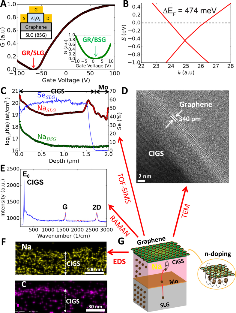
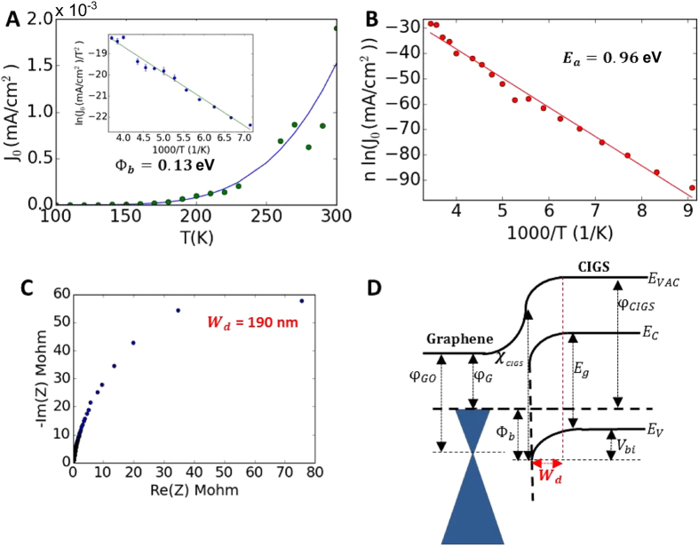
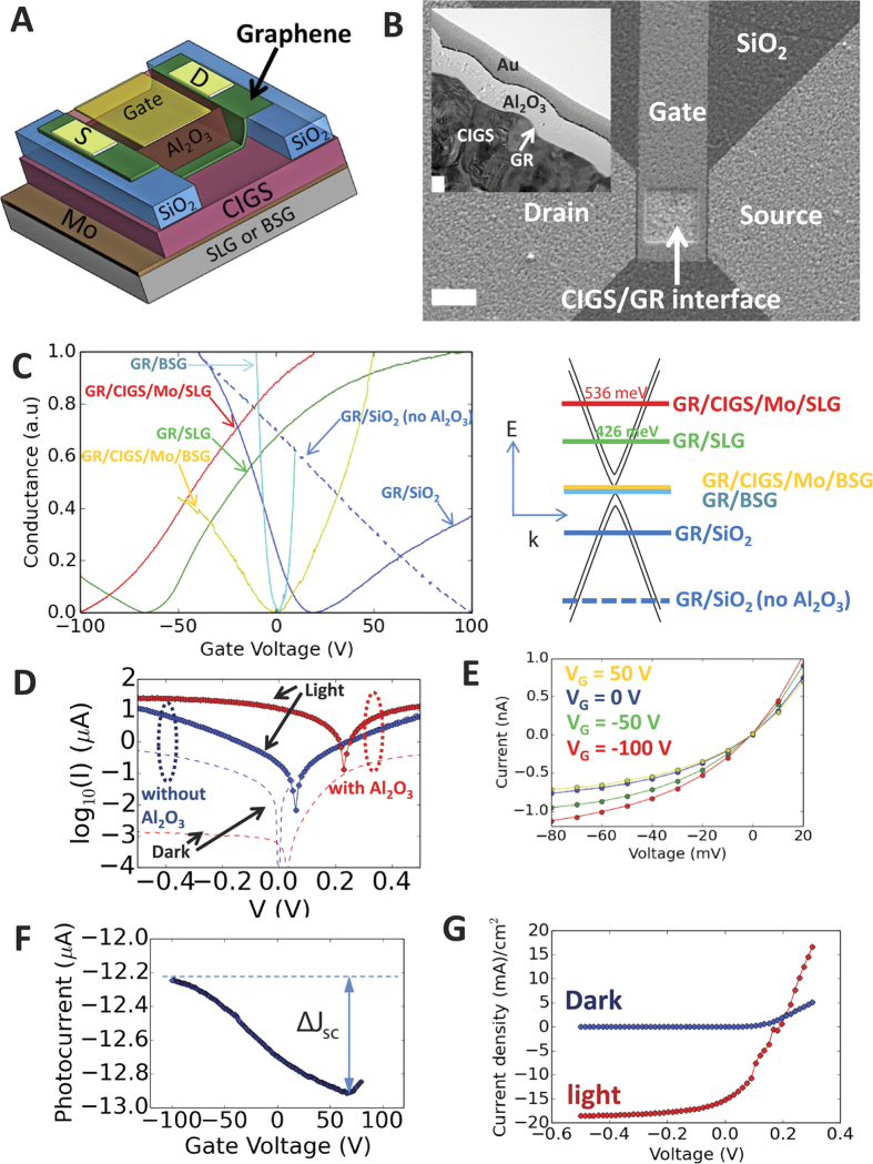
Scalable and low-cost doping of graphene could improve technologies in a wide range of fields such as microelectronics, optoelectronics, and energy storage. While achieving strong p-doping is relatively straightforward, non-electrostatic approaches to n-dope graphene, such as chemical doping, have yielded electron densities of 9.5 × 10(12) e/cm(2) or below. Furthermore, chemical doping is susceptible to degradation and can adversely affect intrinsic graphene's properties. Here we demonstrate strong (1.33 × 10(13) e/cm(2)), robust, and spontaneous graphene n-doping on a soda-lime-glass substrate via surface-transfer doping from Na without any external chemical, high-temperature, or vacuum processes. Remarkably, the n-doping reaches 2.11 × 10(13) e/cm(2) when graphene is transferred onto a p-type copper indium gallium diselenide (CIGS) semiconductor that itself has been deposited onto soda-lime-glass, via surface-transfer doping from Na atoms that diffuse to the CIGS surface. Using this effect, we demonstrate an n-graphene/p-semiconductor Schottky junction with ideality factor of 1.21 and strong photo-response. The ability to achieve strong and persistent graphene n-doping on low-cost, industry-standard materials paves the way toward an entirely new class of graphene-based devices such as photodetectors, photovoltaics, sensors, batteries, and supercapacitors.
可扩展且低成本的石墨烯掺杂能够改善微电子、光电子和能量存储等广泛领域的技术。虽然实现强p型掺杂相对简单,但诸如化学掺杂等非静电方法对石墨烯进行n型掺杂所产生的电子密度为9.5×10¹² e/cm²或更低。此外,化学掺杂容易降解,并且会对本征石墨烯的性能产生不利影响。在此,我们通过来自钠的表面转移掺杂,在钠钙玻璃基板上实现了强(1.33×10¹³ e/cm²)、稳定且自发的石墨烯n型掺杂,无需任何外部化学、高温或真空工艺。值得注意的是,当石墨烯转移到已沉积在钠钙玻璃上的p型铜铟镓硒(CIGS)半导体上时,通过扩散到CIGS表面的钠原子进行表面转移掺杂,n型掺杂达到2.11×10¹³ e/cm²。利用这种效应,我们展示了一个理想因子为1.21且具有强光响应的n型石墨烯/p型半导体肖特基结。在低成本、行业标准材料上实现强而持久的石墨烯n型掺杂的能力,为诸如光电探测器、光伏器件、传感器、电池和超级电容器等全新一类基于石墨烯的器件铺平了道路。