• 文献检索
  • 文档翻译
  • 深度研究
  • 学术资讯
  • Suppr Zotero 插件Zotero 插件
  • 邀请有礼
  • 套餐&价格
  • 历史记录
应用&插件
Suppr Zotero 插件Zotero 插件浏览器插件Mac 客户端Windows 客户端微信小程序
定价
高级版会员购买积分包购买API积分包
服务
文献检索文档翻译深度研究API 文档MCP 服务
关于我们
关于 Suppr公司介绍联系我们用户协议隐私条款
关注我们

Suppr 超能文献

核心技术专利:CN118964589B侵权必究
粤ICP备2023148730 号-1Suppr @ 2026

文献检索

告别复杂PubMed语法,用中文像聊天一样搜索,搜遍4000万医学文献。AI智能推荐,让科研检索更轻松。

立即免费搜索

文件翻译

保留排版,准确专业,支持PDF/Word/PPT等文件格式,支持 12+语言互译。

免费翻译文档

深度研究

AI帮你快速写综述,25分钟生成高质量综述,智能提取关键信息,辅助科研写作。

立即免费体验

在六方氮化硼上生长的二硫化钨原子层中,极低功率密度下的双激子辐射的观测。

Observation of biexcitonic emission at extremely low power density in tungsten disulfide atomic layers grown on hexagonal boron nitride.

机构信息

Department of Chemistry, Nagoya University, Nagoya, 464-8602, Japan.

Institute of Advanced Energy, Kyoto University, Uji, Kyoto, 611-0011, Japan.

出版信息

Sci Rep. 2017 Mar 23;7(1):322. doi: 10.1038/s41598-017-00068-0.

DOI:10.1038/s41598-017-00068-0
PMID:28336931
原文链接:https://pmc.ncbi.nlm.nih.gov/articles/PMC5428332/
Abstract

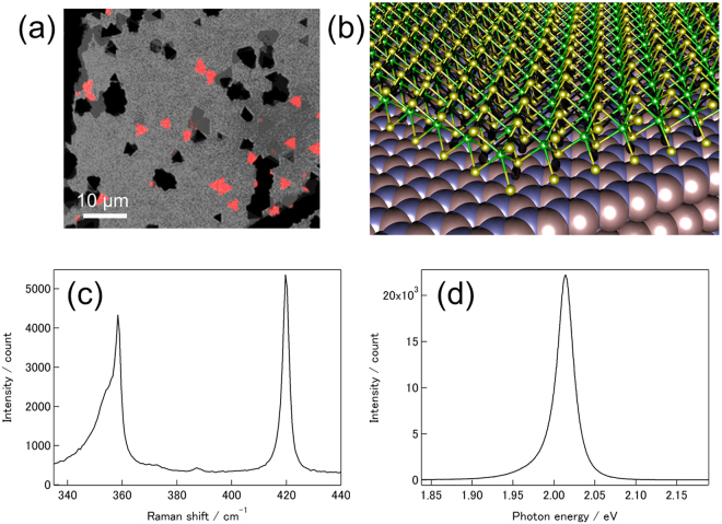
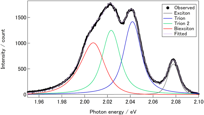
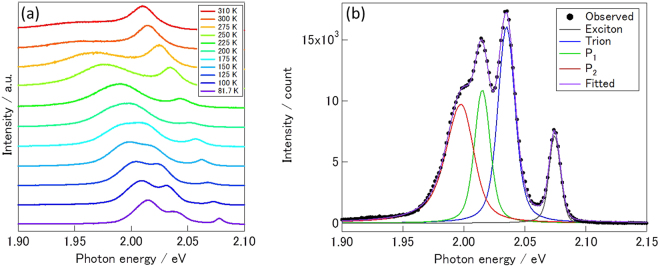
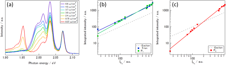
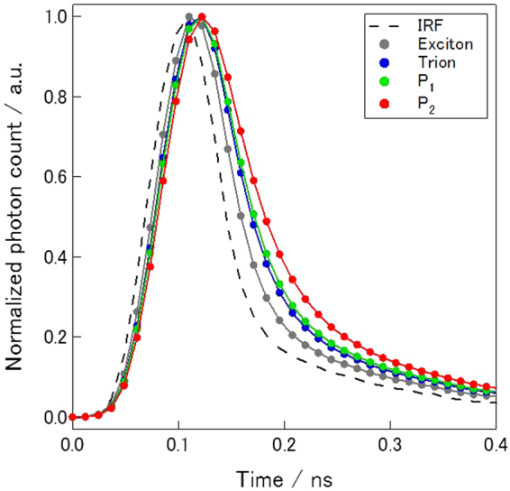
Monolayer transition metal dichalcogenides (TMDCs) including WS, MoS, WSe and WS, are two-dimensional semiconductors with direct bandgap, providing an excellent field for exploration of many-body effects in 2-dimensions (2D) through optical measurements. To fully explore the physics of TMDCs, the prerequisite is preparation of high-quality samples to observe their intrinsic properties. For this purpose, we have focused on high-quality samples, WS grown by chemical vapor deposition method with hexagonal boron nitride as substrates. We observed sharp exciton emissions, whose linewidth is typically 22~23 meV, in photoluminescence spectra at room temperature, which result clearly demonstrates the high-quality of the current samples. We found that biexcitons formed with extremely low-excitation power (240 W/cm) at 80 K, and this should originate from the minimal amount of localization centers in the present high-quality samples. The results clearly demonstrate that the present samples can provide an excellent field, where one can observe various excitonic states, offering possibility of exploring optical physics in 2D and finding new condensates.

摘要

单层过渡金属二卤族化合物(TMDCs)包括 WS、MoS、WSe 和 WS2,是具有直接带隙的二维半导体,通过光学测量为探索二维(2D)中的多体效应提供了极好的领域。为了充分探索 TMDCs 的物理性质,前提是制备高质量的样品以观察其固有特性。为此,我们专注于高质量的样品,即通过化学气相沉积法在六方氮化硼衬底上生长的 WS2。我们在室温下的光致发光光谱中观察到了尖锐的激子发射,其线宽通常为 22~23 meV,这清楚地表明了当前样品的高质量。我们发现双激子在 80 K 时以极低的激发功率(240 W/cm)形成,这应该源于当前高质量样品中最小数量的局域化中心。结果清楚地表明,当前的样品可以提供一个极好的领域,在这个领域中可以观察到各种激子态,为探索二维光学物理和发现新凝聚态提供了可能性。

https://cdn.ncbi.nlm.nih.gov/pmc/blobs/9a31/5428332/144630edac00/41598_2017_68_Fig5_HTML.jpg
https://cdn.ncbi.nlm.nih.gov/pmc/blobs/9a31/5428332/90b03100b7f9/41598_2017_68_Fig1_HTML.jpg
https://cdn.ncbi.nlm.nih.gov/pmc/blobs/9a31/5428332/451d549831cb/41598_2017_68_Fig2_HTML.jpg
https://cdn.ncbi.nlm.nih.gov/pmc/blobs/9a31/5428332/3d6e34e4e3a8/41598_2017_68_Fig3_HTML.jpg
https://cdn.ncbi.nlm.nih.gov/pmc/blobs/9a31/5428332/5bb01fb77929/41598_2017_68_Fig4_HTML.jpg
https://cdn.ncbi.nlm.nih.gov/pmc/blobs/9a31/5428332/144630edac00/41598_2017_68_Fig5_HTML.jpg

相似文献

1
Observation of biexcitonic emission at extremely low power density in tungsten disulfide atomic layers grown on hexagonal boron nitride.在六方氮化硼上生长的二硫化钨原子层中,极低功率密度下的双激子辐射的观测。
Sci Rep. 2017 Mar 23;7(1):322. doi: 10.1038/s41598-017-00068-0.
2
Direct chemical vapor deposition growth of WS2 atomic layers on hexagonal boron nitride.WS2 原子层在六方氮化硼上的直接化学气相沉积生长。
ACS Nano. 2014 Aug 26;8(8):8273-7. doi: 10.1021/nn503093k. Epub 2014 Aug 12.
3
Growth and Optical Properties of High-Quality Monolayer WS2 on Graphite.高质量单层 WS2 在石墨上的生长和光学性质。
ACS Nano. 2015 Apr 28;9(4):4056-63. doi: 10.1021/acsnano.5b00103. Epub 2015 Mar 30.
4
Photoluminescence Segmentation within Individual Hexagonal Monolayer Tungsten Disulfide Domains Grown by Chemical Vapor Deposition.化学气相沉积法生长的单个六方单层二硫化钨域内的光致发光分割。
ACS Appl Mater Interfaces. 2017 May 3;9(17):15005-15014. doi: 10.1021/acsami.6b16287. Epub 2017 Apr 20.
5
Biexciton Formation in Bilayer Tungsten Disulfide.双层二硫化钨中的双激子形成。
ACS Nano. 2016 Feb 23;10(2):2176-83. doi: 10.1021/acsnano.5b06678. Epub 2016 Jan 13.
6
High Luminescence Efficiency in MoS2 Grown by Chemical Vapor Deposition.化学气相沉积法生长的 MoS2 的高光致发光效率。
ACS Nano. 2016 Jul 26;10(7):6535-41. doi: 10.1021/acsnano.6b03443. Epub 2016 Jun 15.
7
Determining the Optimized Interlayer Separation Distance in Vertical Stacked 2D WS :hBN:MoS Heterostructures for Exciton Energy Transfer.确定用于激子能量转移的垂直堆叠二维WS:hBN:MoS异质结构中的优化层间分离距离
Small. 2018 Mar;14(13):e1703727. doi: 10.1002/smll.201703727. Epub 2018 Feb 7.
8
Resolidified Chalcogen Precursors for High-Quality 2D Semiconductor Growth.用于高质量二维半导体生长的再凝固硫属元素前体。
Angew Chem Int Ed Engl. 2023 Jul 17;62(29):e202301501. doi: 10.1002/anie.202301501. Epub 2023 Apr 28.
9
High-mobility and air-stable single-layer WS2 field-effect transistors sandwiched between chemical vapor deposition-grown hexagonal BN films.夹在化学气相沉积生长的六方氮化硼薄膜之间的高迁移率且空气稳定的单层二硫化钨场效应晶体管。
Sci Rep. 2015 Jun 1;5:10699. doi: 10.1038/srep10699.
10
Study on the Growth Parameters and the Electrical and Optical Behaviors of 2D Tungsten Disulfide.二维二硫化钨的生长参数及电学和光学行为研究
ACS Appl Mater Interfaces. 2020 Apr 8;12(14):16576-16583. doi: 10.1021/acsami.9b19820. Epub 2020 Mar 26.

引用本文的文献

1
Theory of Excitons in Atomically Thin Semiconductors: Tight-Binding Approach.原子级薄半导体中的激子理论:紧束缚方法。
Nanomaterials (Basel). 2022 May 6;12(9):1582. doi: 10.3390/nano12091582.
2
Dark-exciton valley dynamics in transition metal dichalcogenide alloy monolayers.过渡金属二硫族化物合金单层中的暗激子谷动力学
Sci Rep. 2019 Mar 14;9(1):4575. doi: 10.1038/s41598-019-40932-9.
3
Revealing the biexciton and trion-exciton complexes in BN encapsulated WSe.揭示 BN 封装 WSe 中的双激子和三激子-激子复合物

本文引用的文献

1
Biexciton Formation in Bilayer Tungsten Disulfide.双层二硫化钨中的双激子形成。
ACS Nano. 2016 Feb 23;10(2):2176-83. doi: 10.1021/acsnano.5b06678. Epub 2016 Jan 13.
2
Biexciton Emission from Edges and Grain Boundaries of Triangular WS₂ Monolayers.三角形 WS₂ 单层边缘和晶界的双激子发射。
ACS Nano. 2016 Feb 23;10(2):2399-405. doi: 10.1021/acsnano.5b07214. Epub 2016 Jan 15.
3
Large-area synthesis of high-quality and uniform monolayer WS2 on reusable Au foils.在可重复使用的金箔上大面积合成高质量且均匀的单层二硫化钨。
Nat Commun. 2018 Sep 13;9(1):3719. doi: 10.1038/s41467-018-05863-5.
Nat Commun. 2015 Oct 9;6:8569. doi: 10.1038/ncomms9569.
4
Direct Growth of Single- and Few-Layer MoS2 on h-BN with Preferred Relative Rotation Angles.单层和少层 MoS2 在具有优选相对旋转角度的 h-BN 上的直接生长。
Nano Lett. 2015 Oct 14;15(10):6324-31. doi: 10.1021/acs.nanolett.5b01311. Epub 2015 Sep 14.
5
Synthesis and Transfer of Large-Area Monolayer WS2 Crystals: Moving Toward the Recyclable Use of Sapphire Substrates.大面积单层 WS2 晶体的合成与转移:迈向蓝宝石衬底可回收利用的目标。
ACS Nano. 2015 Jun 23;9(6):6178-87. doi: 10.1021/acsnano.5b01480. Epub 2015 May 15.
6
All Chemical Vapor Deposition Growth of MoS2:h-BN Vertical van der Waals Heterostructures.MoS2:h-BN 垂直范德华异质结构的所有化学气相沉积生长。
ACS Nano. 2015 May 26;9(5):5246-54. doi: 10.1021/acsnano.5b00655. Epub 2015 Apr 20.
7
Exciton binding energy of monolayer WS₂.单层WS₂的激子结合能。
Sci Rep. 2015 Mar 18;5:9218. doi: 10.1038/srep09218.
8
Observation of excitonic fine structure in a 2D transition-metal dichalcogenide semiconductor.二维过渡金属二卤族半导体中激子精细结构的观测。
ACS Nano. 2015 Jan 27;9(1):647-55. doi: 10.1021/nn5059908. Epub 2015 Jan 12.
9
Ultrafast dynamics of defect-assisted electron-hole recombination in monolayer MoS2.单层 MoS2 中缺陷辅助的电子-空穴复合超快动力学。
Nano Lett. 2015 Jan 14;15(1):339-45. doi: 10.1021/nl503636c. Epub 2014 Dec 31.
10
Photonic architectures for equilibrium high-temperature Bose-Einstein condensation in dichalcogenide monolayers.用于二硫化物单层中平衡高温玻色-爱因斯坦凝聚的光子架构。
Sci Rep. 2014 Dec 11;4:7432. doi: 10.1038/srep07432.