Iqbal M Waqas, Iqbal M Zahir, Khan M Farooq, Shehzad M Arslan, Seo Yongho, Park Jong Hyun, Hwang Chanyong, Eom Jonghwa
Department of Physics and Graphene Research Institute, Sejong University, Seoul 143-747, Korea.
Faculty of Nanotechnology &Advanced Materials Engineering and Graphene Research Institute, Sejong University, Seoul 143-747, Korea.
Sci Rep. 2015 Jun 1;5:10699. doi: 10.1038/srep10699.
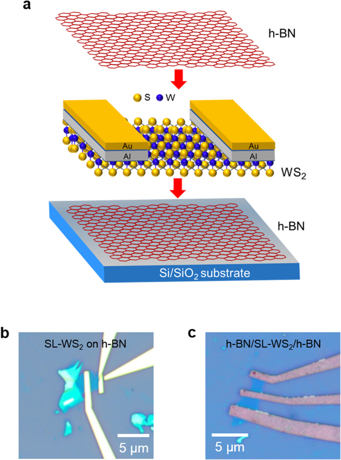
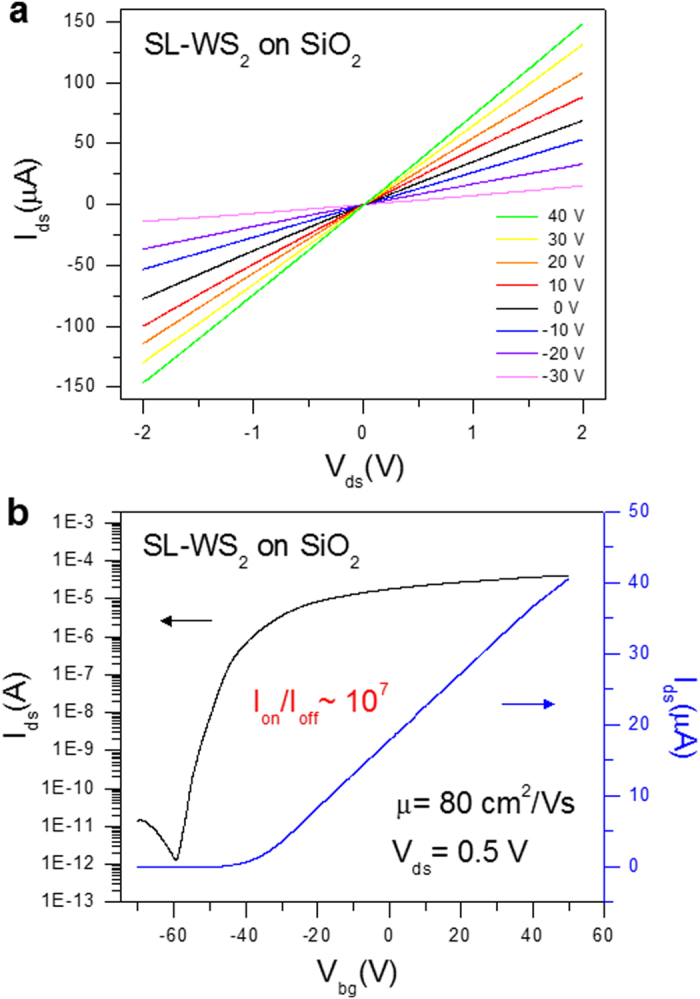
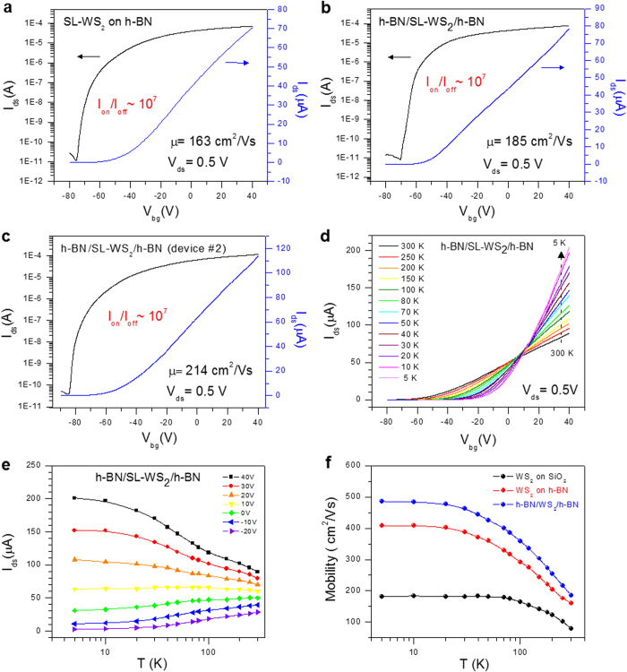
An emerging electronic material as one of transition metal dichalcogenides (TMDCs), tungsten disulfide (WS2) can be exfoliated as an atomically thin layer and can compensate for the drawback of graphene originating from a gapless band structure. A direct bandgap, which is obtainable in single-layer WS2, is an attractive characteristic for developing optoelectronic devices, as well as field-effect transistors. However, its relatively low mobility and electrical characteristics susceptible to environments remain obstacles for the use of device materials. Here, we demonstrate remarkable improvement in the electrical characteristics of single-layer WS2 field-effect transistor (SL-WS2 FET) using chemical vapor deposition (CVD)-grown hexagonal BN (h-BN). SL-WS2 FET sandwiched between CVD-grown h-BN films shows unprecedented high mobility of 214 cm(2)/Vs at room temperature. The mobility of a SL-WS2 FET has been found to be 486 cm(2)/Vs at 5 K. The ON/OFF ratio of output current is ~10(7) at room temperature. Apart from an ideal substrate for WS2 FET, CVD-grown h-BN film also provides a protection layer against unwanted influence by gas environments. The h-BN/SL-WS2/h-BN sandwich structure offers a way to develop high-quality durable single-layer TMDCs electronic devices.
作为过渡金属二硫属化物(TMDCs)之一的新兴电子材料二硫化钨(WS2),可以被剥离成原子级的薄层,并且能够弥补源于无带隙能带结构的石墨烯的缺点。单层WS2中可获得的直接带隙,对于开发光电器件以及场效应晶体管来说是一个有吸引力的特性。然而,其相对较低的迁移率以及易受环境影响的电学特性,仍然是其作为器件材料应用的障碍。在此,我们展示了使用化学气相沉积(CVD)生长的六方氮化硼(h-BN),单层WS2场效应晶体管(SL-WS2 FET)的电学特性有了显著改善。夹在CVD生长的h-BN薄膜之间的SL-WS2 FET在室温下展现出前所未有的214 cm²/Vs的高迁移率。已发现SL-WS2 FET在5 K时的迁移率为486 cm²/Vs。输出电流的开/关比在室温下约为10⁷。除了是WS2 FET的理想衬底外,CVD生长的h-BN薄膜还提供了一个保护层,可抵御气体环境的不良影响。h-BN/SL-WS2/h-BN三明治结构为开发高质量耐用的单层TMDCs电子器件提供了一种方法。