Solar Energy & Advanced Materials Research Group, Department of Chemical Engineering, UCL, Torrington Place, London, WC1E 7JE, UK.
Key Laboratory of Flexible Electronics (KLOFE) & Institute of Advanced Materials (IAM), Jiangsu National Synergetic Innovation Center for Advanced Materials (SICAM), Nanjing Tech University (NanjingTech), 30 South Puzhu Road, Nanjing, 211816, P.R. China.
Angew Chem Int Ed Engl. 2017 Jul 3;56(28):8221-8225. doi: 10.1002/anie.201703372. Epub 2017 Jun 12.
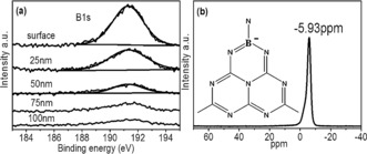
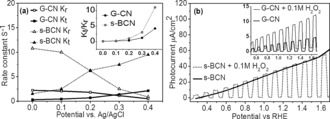
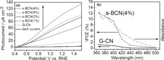
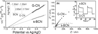
A metal-free photoanode nanojunction architecture, composed of B-doped carbon nitride nanolayer and bulk carbon nitride, was fabricated by a one-step approach. This type of nanojunction (s-BCN) overcomes a few intrinsic drawbacks of carbon nitride film (severe bulk charge recombination and slow charge transfer). The top layer of the nanojunction has a depth of ca. 100 nm and the bottom layer is ca. 900 nm. The nanojunction photoanode results into a 10-fold higher photocurrent than bulk graphitic carbon nitride (G-CN) photoanode, with a record photocurrent density of 103.2 μA cm at 1.23 V vs. RHE under one sun irradiation and an extremely high incident photon-to-current efficiency (IPCE) of ca. 10 % at 400 nm. Electrochemical impedance spectroscopy, Mott-Schottky plots, and intensity-modulated photocurrent spectroscopy show that such enhancement is mainly due to the mitigated deep trap states, a more than 10 times faster charge transfer rate and nearly three times higher conductivity due to the nanojunction architecture.
一种由 B 掺杂氮化碳纳米层和块状氮化碳组成的无金属光阴极纳米结结构,通过一步法制备。这种纳米结(s-BCN)克服了氮化碳薄膜的一些内在缺陷(严重的体相电荷复合和缓慢的电荷转移)。纳米结的顶层深度约为 100nm,底层深度约为 900nm。与块状石墨相氮化碳(G-CN)光阳极相比,纳米结光阳极的光电流提高了 10 倍,在 1.23V 相对于 RHE 的 1 个太阳辐照下,光电流密度达到 103.2μA cm,在 400nm 时的光生载流子量子效率(IPCE)极高,约为 10%。电化学阻抗谱、Mott-Schottky 图和强度调制光电流谱表明,这种增强主要归因于深陷阱态的缓解、10 倍以上的电荷转移速率以及由于纳米结结构导致的近 3 倍的电导率提高。