Center for Nanophotonics, AMOLF , Science Park 104, 1098 XG Amsterdam, The Netherlands.
Nano Lett. 2017 Sep 13;17(9):5206-5212. doi: 10.1021/acs.nanolett.7b01092. Epub 2017 Aug 16.
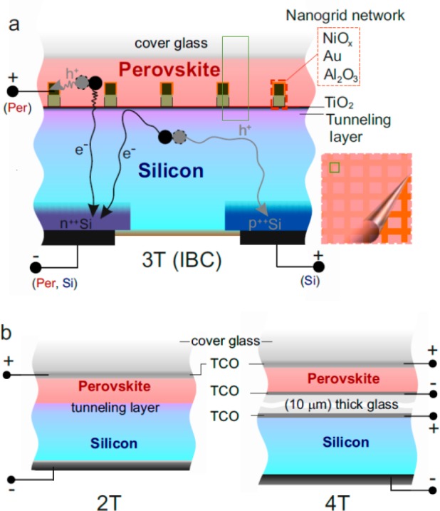
Tandem photovoltaics, combining absorber layers with two distinct band gap energies into a single device, provide a practical solution to reduce thermalization losses in solar energy conversion. Traditionally, tandem devices have been assembled using two-terminal (2-T) or four-terminal (4-T) configurations; the 2-T limits the tandem performance due to the series connection requiring current matching, while the standard 4-T configuration requires at least three transparent electrical contacts, which reduce the total collected power due to unavoidable parasitic absorption. Here, we introduce a novel architecture based on a nanoscale back-contact for a thin-film top cell in a three terminal (3-T) configuration. Using coupled optical-electrical modeling, we optimize this architecture for a planar perovskite-silicon tandem, highlighting the roles of nanoscale contacts to reduce the required perovskite electronic quality. For example, with an 18% planar silicon base cell, the 3-T back contact design can reach a 32.9% tandem efficiency with a 10 μm diffusion length perovskite material. Using the same perovskite quality, the 4-T and 2-T configurations only reach 30.2% and 24.8%, respectively. We also confirm that the same 3-T efficiency advantage applies when using 25% efficient textured silicon base cells, where the tandems reach 35.2% and 32.8% efficiency for the 3-T, and 4-T configurations, respectively. Furthermore, because our design is based on the individual subcells being back-contacted, further improvements can be readily made by optimizing the front surface, which is left free for additional antireflective coating, light trapping, surface passivation, and photoluminescence outcoupling enhancements.
串联光伏,将具有两个不同带隙能量的吸收层组合到单个器件中,为减少太阳能转换中的热化损失提供了一种实用的解决方案。传统上,串联器件采用二端(2-T)或四端(4-T)配置进行组装;由于串联需要电流匹配,2-T 限制了串联性能,而标准的 4-T 配置至少需要三个透明电接触,由于不可避免的寄生吸收,这会降低总收集功率。在这里,我们引入了一种基于纳米级背接触的新型架构,用于三端(3-T)配置的薄膜顶电池。使用耦合光电建模,我们针对平面钙钛矿-硅串联结构对该架构进行了优化,强调了纳米级接触在降低所需钙钛矿电子质量方面的作用。例如,对于 18%的平面硅基电池,3-T 背接触设计可以使用 10 μm 扩散长度的钙钛矿材料达到 32.9%的串联效率。使用相同的钙钛矿质量,4-T 和 2-T 配置分别只能达到 30.2%和 24.8%。我们还证实,当使用 25%效率的织构化硅基电池时,相同的 3-T 效率优势也适用,其中 3-T 和 4-T 配置的串联效率分别达到 35.2%和 32.8%。此外,由于我们的设计基于各个子电池的背接触,因此可以通过优化前表面轻松实现进一步改进,前表面可自由用于额外的抗反射涂层、光捕获、表面钝化和光致发光外耦合增强。