• 文献检索
  • 文档翻译
  • 深度研究
  • 学术资讯
  • Suppr Zotero 插件Zotero 插件
  • 邀请有礼
  • 套餐&价格
  • 历史记录
应用&插件
Suppr Zotero 插件Zotero 插件浏览器插件Mac 客户端Windows 客户端微信小程序
定价
高级版会员购买积分包购买API积分包
服务
文献检索文档翻译深度研究API 文档MCP 服务
关于我们
关于 Suppr公司介绍联系我们用户协议隐私条款
关注我们

Suppr 超能文献

核心技术专利:CN118964589B侵权必究
粤ICP备2023148730 号-1Suppr @ 2026

文献检索

告别复杂PubMed语法,用中文像聊天一样搜索,搜遍4000万医学文献。AI智能推荐,让科研检索更轻松。

立即免费搜索

文件翻译

保留排版,准确专业,支持PDF/Word/PPT等文件格式,支持 12+语言互译。

免费翻译文档

深度研究

AI帮你快速写综述,25分钟生成高质量综述,智能提取关键信息,辅助科研写作。

立即免费体验

一硫化钐(SmS):性质与应用综述

Samarium Monosulfide (SmS): Reviewing Properties and Applications.

作者信息

Sousanis Andreas, Smet Philippe F, Poelman Dirk

机构信息

Lumilab, Department of Solid State Sciences, Ghent University, Krijgslaan 281/S1, 9000 Gent, Belgium.

出版信息

Materials (Basel). 2017 Aug 16;10(8):953. doi: 10.3390/ma10080953.

DOI:10.3390/ma10080953
PMID:28813006
原文链接:https://pmc.ncbi.nlm.nih.gov/articles/PMC5578319/
Abstract

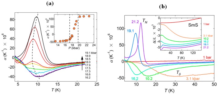
In this review, we give an overview of the properties and applications of samarium monosulfide, SmS, which has gained considerable interest as a switchable material. It shows a pressure-induced phase transition from the semiconducting to the metallic state by polishing, and it switches back to the semiconducting state by heating. The material also shows a magnetic transition, from the paramagnetic state to an antiferromagnetically ordered state. The switching behavior between the semiconducting and metallic states could be exploited in several applications, such as high density optical storage and memory materials, thermovoltaic devices, infrared sensors and more. We discuss the electronic, optical and magnetic properties of SmS, its switching behavior, as well as the thin film deposition techniques which have been used, such as e-beam evaporation and sputtering. Moreover, applications and possible ideas for future work on this material are presented. Our scope is to present the properties of SmS, which were mainly measured in bulk crystals, while at the same time we describe the possible deposition methods that will push the study of SmS to nanoscale dimensions, opening an intriguing range of applications for low-dimensional, pressure-induced semiconductor-metal transition compounds.

摘要

在本综述中,我们概述了一硫化钐(SmS)的性质和应用,它作为一种可切换材料已引起了广泛关注。通过抛光,它会发生压力诱导的从半导体态到金属态的相变,而通过加热又会变回半导体态。该材料还表现出磁转变,从顺磁态转变为反铁磁有序态。半导体态和金属态之间的切换行为可应用于多种领域,如高密度光存储和记忆材料、热光伏器件、红外传感器等。我们讨论了SmS的电子、光学和磁性质、其切换行为,以及所使用的薄膜沉积技术,如电子束蒸发和溅射。此外,还介绍了该材料的应用以及未来工作的可能思路。我们的目的是介绍主要在块状晶体中测量的SmS的性质,同时描述可能的沉积方法,这些方法将推动SmS的研究进入纳米尺度,为低维、压力诱导的半导体 - 金属转变化合物开启一系列有趣的应用。

https://cdn.ncbi.nlm.nih.gov/pmc/blobs/d170/5578319/c42fb4ed91f6/materials-10-00953-g012.jpg
https://cdn.ncbi.nlm.nih.gov/pmc/blobs/d170/5578319/19bea6aa1b05/materials-10-00953-g001.jpg
https://cdn.ncbi.nlm.nih.gov/pmc/blobs/d170/5578319/85b854a05f46/materials-10-00953-g002.jpg
https://cdn.ncbi.nlm.nih.gov/pmc/blobs/d170/5578319/1e4434602d9c/materials-10-00953-g003.jpg
https://cdn.ncbi.nlm.nih.gov/pmc/blobs/d170/5578319/ec476d5166b9/materials-10-00953-g004.jpg
https://cdn.ncbi.nlm.nih.gov/pmc/blobs/d170/5578319/f43d89efbbcd/materials-10-00953-g005.jpg
https://cdn.ncbi.nlm.nih.gov/pmc/blobs/d170/5578319/20d0ce5580e3/materials-10-00953-g006.jpg
https://cdn.ncbi.nlm.nih.gov/pmc/blobs/d170/5578319/ab0d45816945/materials-10-00953-g007.jpg
https://cdn.ncbi.nlm.nih.gov/pmc/blobs/d170/5578319/43426b6170ba/materials-10-00953-g008.jpg
https://cdn.ncbi.nlm.nih.gov/pmc/blobs/d170/5578319/1816c5ab7f52/materials-10-00953-g009.jpg
https://cdn.ncbi.nlm.nih.gov/pmc/blobs/d170/5578319/3ea46374f239/materials-10-00953-g010.jpg
https://cdn.ncbi.nlm.nih.gov/pmc/blobs/d170/5578319/06b9928ac638/materials-10-00953-g011.jpg
https://cdn.ncbi.nlm.nih.gov/pmc/blobs/d170/5578319/c42fb4ed91f6/materials-10-00953-g012.jpg

相似文献

1
Samarium Monosulfide (SmS): Reviewing Properties and Applications.一硫化钐(SmS):性质与应用综述
Materials (Basel). 2017 Aug 16;10(8):953. doi: 10.3390/ma10080953.
2
Switchable Piezoresistive SmS Thin Films on Large Area.大面积可切换压阻式 SmS 薄膜。
Sensors (Basel). 2019 Oct 11;19(20):4390. doi: 10.3390/s19204390.
3
The thermally induced metal-semiconducting phase transition of samarium monosulfide (SmS) thin films.硫化钐(SmS)薄膜的热致金属-半导体相转变。
J Phys Condens Matter. 2010 Jan 13;22(1):015005. doi: 10.1088/0953-8984/22/1/015005. Epub 2009 Dec 3.
4
SmS/EuS/SmS Tri-Layer Thin Films: The Role of Diffusion in the Pressure Triggered Semiconductor-Metal Transition.硫化钐/硫化铕/硫化钐三层薄膜:扩散在压力触发的半导体-金属转变中的作用
Nanomaterials (Basel). 2019 Oct 24;9(11):1513. doi: 10.3390/nano9111513.
5
Optical properties of vanadium dioxide and vanadium pentoxide thin films.二氧化钒和五氧化二钒薄膜的光学性质。
Appl Opt. 1991 Jul 1;30(19):2782-7. doi: 10.1364/AO.30.002782.
6
Electronic structure and optical signatures of semiconducting transition metal dichalcogenide nanosheets.半导体过渡金属二卤化物纳米片的电子结构和光学特征。
Acc Chem Res. 2015 Jan 20;48(1):91-9. doi: 10.1021/ar500303m. Epub 2014 Dec 17.
7
Transparent ferromagnetic and semiconducting behavior in Fe-Dy-Tb based amorphous oxide films.基于铁-镝-铽的非晶氧化物薄膜中的透明铁磁和半导体行为。
Sci Rep. 2016 Jun 14;6:27869. doi: 10.1038/srep27869.
8
Improved VO(2) thin films for infrared switching.用于红外开关的改进型VO(2)薄膜。
Appl Opt. 1991 Oct 1;30(28):4119-23. doi: 10.1364/AO.30.004119.
9
[Electrical and optical phase transition properties of nano vanadium dioxide thin films].[纳米二氧化钒薄膜的电学和光学相变特性]
Guang Pu Xue Yu Guang Pu Fen Xi. 2010 Apr;30(4):1002-7.
10
Networks of semiconducting SWNTs: contribution of midgap electronic states to the electrical transport.半导体 SWNTs 网络: 能隙中间电子态对输运性质的贡献。
Acc Chem Res. 2015 Aug 18;48(8):2270-9. doi: 10.1021/acs.accounts.5b00107. Epub 2015 Aug 5.

引用本文的文献

1
Tunable valence tautomerism in lanthanide-organic alloys.镧系有机合金中的可调价互变异构现象。
Nat Chem. 2024 May;16(5):735-740. doi: 10.1038/s41557-023-01422-8. Epub 2024 Feb 19.
2
Thorium and Rare Earth Monoxides and Related Phases.钍和稀土单氧化物及相关物相。
Materials (Basel). 2023 Feb 5;16(4):1350. doi: 10.3390/ma16041350.
3
Probing FeSi, a -electron topological Kondo insulator candidate, with magnetic field, pressure, and microwaves.用磁场、压力和微波探测 FeSi,一种 - 电子拓扑 Kondo 绝缘体候选材料。

本文引用的文献

1
Surface-dominated conduction up to 240 K in the Kondo insulator SmB under strain.应变下近藤绝缘体SmB中高达240K的表面主导传导。
Nat Mater. 2017 Jul;16(7):708-711. doi: 10.1038/nmat4888. Epub 2017 Apr 3.
2
Topological Properties and the Dynamical Crossover from Mixed-Valence to Kondo-Lattice Behavior in the Golden Phase of SmS.SmS金相中混合价态到近藤晶格行为的拓扑性质及动力学转变
Phys Rev Lett. 2015 Apr 24;114(16):166404. doi: 10.1103/PhysRevLett.114.166404. Epub 2015 Apr 22.
3
Overview of emerging nonvolatile memory technologies.
Proc Natl Acad Sci U S A. 2023 Feb 21;120(8):e2216367120. doi: 10.1073/pnas.2216367120. Epub 2023 Feb 15.
4
Nanotubes from the Misfit Layered Compound (SmS)TaS: Atomic Structure, Charge Transfer, and Electrical Properties.来自错配层状化合物(SmS)TaS的纳米管:原子结构、电荷转移和电学性质。
Chem Mater. 2022 Feb 22;34(4):1838-1853. doi: 10.1021/acs.chemmater.1c04106. Epub 2022 Feb 10.
5
SmS/EuS/SmS Tri-Layer Thin Films: The Role of Diffusion in the Pressure Triggered Semiconductor-Metal Transition.硫化钐/硫化铕/硫化钐三层薄膜:扩散在压力触发的半导体-金属转变中的作用
Nanomaterials (Basel). 2019 Oct 24;9(11):1513. doi: 10.3390/nano9111513.
6
Switchable Piezoresistive SmS Thin Films on Large Area.大面积可切换压阻式 SmS 薄膜。
Sensors (Basel). 2019 Oct 11;19(20):4390. doi: 10.3390/s19204390.
新兴非易失性存储技术概述。
Nanoscale Res Lett. 2014 Sep 25;9(1):526. doi: 10.1186/1556-276X-9-526. eCollection 2014.
4
Topological surface state in the Kondo insulator samarium hexaboride.拓扑表面态在 Kondo 绝缘的六硼化钐中。
Nat Mater. 2014 May;13(5):466-70. doi: 10.1038/nmat3913. Epub 2014 Mar 23.
5
Giant piezoresistive on/off ratios in rare-earth chalcogenide thin films enabling nanomechanical switching.稀土地属硫族化物薄膜中的巨大压阻式 ON/OFF 比,实现纳米机械开关。
Nano Lett. 2013 Oct 9;13(10):4650-3. doi: 10.1021/nl401710f. Epub 2013 Sep 12.
6
Experimental study of the 4fn → 4fn and 4fn → 4fn-15d1 transitions of the lanthanide diiodides LnI2 (Ln=Nd, Sm, Eu, Dy, Tm, Yb).镧系二碘化合物 LnI2(Ln=Nd、Sm、Eu、Dy、Tm、Yb)的 4fn → 4fn 和 4fn → 4fn-15d1 跃迁的实验研究。
J Phys Condens Matter. 2012 Jul 11;24(27):275502. doi: 10.1088/0953-8984/24/27/275502. Epub 2012 Jun 20.
7
Design rules for phase-change materials in data storage applications.用于数据存储应用的相变材料的设计规则。
Adv Mater. 2011 May 10;23(18):2030-58. doi: 10.1002/adma.201004255. Epub 2011 Apr 5.
8
The thermally induced metal-semiconducting phase transition of samarium monosulfide (SmS) thin films.硫化钐(SmS)薄膜的热致金属-半导体相转变。
J Phys Condens Matter. 2010 Jan 13;22(1):015005. doi: 10.1088/0953-8984/22/1/015005. Epub 2009 Dec 3.
9
A map for phase-change materials.一张用于相变材料的图谱。
Nat Mater. 2008 Dec;7(12):972-7. doi: 10.1038/nmat2330. Epub 2008 Nov 16.
10
Pressure-induced magnetic order in golden SmS.
Phys Rev Lett. 2004 Feb 13;92(6):066401. doi: 10.1103/PhysRevLett.92.066401.