• 文献检索
  • 文档翻译
  • 深度研究
  • 学术资讯
  • Suppr Zotero 插件Zotero 插件
  • 邀请有礼
  • 套餐&价格
  • 历史记录
应用&插件
Suppr Zotero 插件Zotero 插件浏览器插件Mac 客户端Windows 客户端微信小程序
定价
高级版会员购买积分包购买API积分包
服务
文献检索文档翻译深度研究API 文档MCP 服务
关于我们
关于 Suppr公司介绍联系我们用户协议隐私条款
关注我们

Suppr 超能文献

核心技术专利:CN118964589B侵权必究
粤ICP备2023148730 号-1Suppr @ 2026

文献检索

告别复杂PubMed语法,用中文像聊天一样搜索,搜遍4000万医学文献。AI智能推荐,让科研检索更轻松。

立即免费搜索

文件翻译

保留排版,准确专业,支持PDF/Word/PPT等文件格式,支持 12+语言互译。

免费翻译文档

深度研究

AI帮你快速写综述,25分钟生成高质量综述,智能提取关键信息,辅助科研写作。

立即免费体验

全喷墨打印二维材料范德瓦尔斯异质结用于可穿戴和纺织电子产品。

Fully inkjet-printed two-dimensional material field-effect heterojunctions for wearable and textile electronics.

机构信息

Cambridge Graphene Centre, University of Cambridge, 9 JJ Thomson Avenue, Cambridge, CB3 0FA, UK.

Department of Materials Science and Metallurgy, University of Cambridge, 27 Charles Babbage road, Cambridge, CB3 0FS, UK.

出版信息

Nat Commun. 2017 Oct 31;8(1):1202. doi: 10.1038/s41467-017-01210-2.

DOI:10.1038/s41467-017-01210-2
PMID:29089495
原文链接:https://pmc.ncbi.nlm.nih.gov/articles/PMC5663939/
Abstract

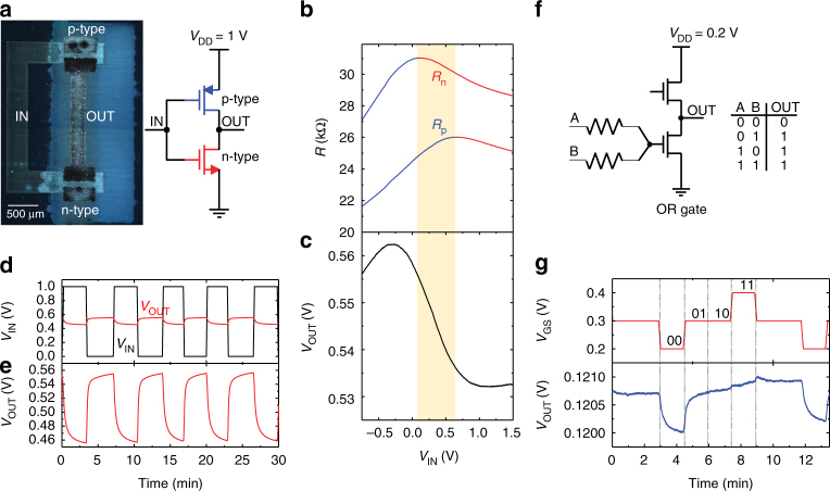
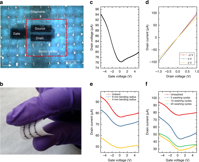
Fully printed wearable electronics based on two-dimensional (2D) material heterojunction structures also known as heterostructures, such as field-effect transistors, require robust and reproducible printed multi-layer stacks consisting of active channel, dielectric and conductive contact layers. Solution processing of graphite and other layered materials provides low-cost inks enabling printed electronic devices, for example by inkjet printing. However, the limited quality of the 2D-material inks, the complexity of the layered arrangement, and the lack of a dielectric 2D-material ink able to operate at room temperature, under strain and after several washing cycles has impeded the fabrication of electronic devices on textile with fully printed 2D heterostructures. Here we demonstrate fully inkjet-printed 2D-material active heterostructures with graphene and hexagonal-boron nitride (h-BN) inks, and use them to fabricate all inkjet-printed flexible and washable field-effect transistors on textile, reaching a field-effect mobility of ~91 cm V s, at low voltage (<5 V). This enables fully inkjet-printed electronic circuits, such as reprogrammable volatile memory cells, complementary inverters and OR logic gates.

摘要

基于二维(2D)材料异质结结构(也称为异质结构)的全印刷可穿戴电子产品,例如场效应晶体管,需要由活性通道、介电层和导电接触层组成的稳健且可重复的印刷多层堆叠。石墨和其他层状材料的溶液处理提供了低成本的油墨,从而能够制造印刷电子产品,例如通过喷墨印刷。然而,二维材料油墨的质量有限、层状排列的复杂性以及缺乏能够在室温下、应变下和经过几次洗涤循环后工作的介电二维材料油墨,阻碍了具有全印刷二维异质结构的纺织品上电子器件的制造。在这里,我们展示了使用石墨烯和六方氮化硼(h-BN)油墨完全喷墨打印的 2D 材料活性异质结构,并使用它们在纺织品上制造了所有喷墨打印的柔性和可清洗场效应晶体管,达到了约 91 cm V s 的场效应迁移率,在低电压(<5 V)下。这使得全喷墨打印的电子电路成为可能,例如可重编程的易失性存储单元、互补反相器和 OR 逻辑门。

https://cdn.ncbi.nlm.nih.gov/pmc/blobs/a514/5663939/8331f73ea979/41467_2017_1210_Fig6_HTML.jpg
https://cdn.ncbi.nlm.nih.gov/pmc/blobs/a514/5663939/5175ed437ad7/41467_2017_1210_Fig1_HTML.jpg
https://cdn.ncbi.nlm.nih.gov/pmc/blobs/a514/5663939/6332fb66d4ba/41467_2017_1210_Fig2_HTML.jpg
https://cdn.ncbi.nlm.nih.gov/pmc/blobs/a514/5663939/3898617cf60e/41467_2017_1210_Fig3_HTML.jpg
https://cdn.ncbi.nlm.nih.gov/pmc/blobs/a514/5663939/e8f4b653a483/41467_2017_1210_Fig4_HTML.jpg
https://cdn.ncbi.nlm.nih.gov/pmc/blobs/a514/5663939/ad11174ee058/41467_2017_1210_Fig5_HTML.jpg
https://cdn.ncbi.nlm.nih.gov/pmc/blobs/a514/5663939/8331f73ea979/41467_2017_1210_Fig6_HTML.jpg

相似文献

1
Fully inkjet-printed two-dimensional material field-effect heterojunctions for wearable and textile electronics.全喷墨打印二维材料范德瓦尔斯异质结用于可穿戴和纺织电子产品。
Nat Commun. 2017 Oct 31;8(1):1202. doi: 10.1038/s41467-017-01210-2.
2
All-2D Material Inkjet-Printed Capacitors: Toward Fully Printed Integrated Circuits.全二维材料喷墨打印电容器:迈向全印刷集成电路。
ACS Nano. 2019 Jan 22;13(1):54-60. doi: 10.1021/acsnano.8b06464. Epub 2018 Nov 27.
3
Inkjet-Printed Molybdenum Disulfide and Nitrogen-Doped Graphene Active Layer High On/Off Ratio Transistors.喷墨打印的二硫化钼和氮掺杂石墨烯有源层高开关比晶体管。
Molecules. 2020 Feb 28;25(5):1081. doi: 10.3390/molecules25051081.
4
Barium titanate-enhanced hexagonal boron nitride inks for printable high-performance dielectrics.用于可印刷高性能电介质的钛酸钡增强六方氮化硼油墨。
Nanotechnology. 2022 Mar 4;33(21). doi: 10.1088/1361-6528/ac553f.
5
Water-based 2-dimensional anatase TiO inks for printed diodes and transistors.用于打印二极管和晶体管的水基二维锐钛矿 TiO 油墨。
Nanoscale. 2023 Mar 23;15(12):5689-5695. doi: 10.1039/d2nr05786g.
6
Inkjet-printed h-BN memristors for hardware security.喷墨打印六方氮化硼忆阻器用于硬件安全。
Nanoscale. 2023 Jun 15;15(23):9985-9992. doi: 10.1039/d3nr00030c.
7
All Inkjet-Printed Graphene-Silver Composite Ink on Textiles for Highly Conductive Wearable Electronics Applications.用于高导电性可穿戴电子应用的纺织品上的所有喷墨打印石墨烯-银复合墨水。
Sci Rep. 2019 May 29;9(1):8035. doi: 10.1038/s41598-019-44420-y.
8
Inkjet-Printed, High-Performance MoS Transistors and Unipolar Logic Electronics.喷墨打印的高性能二硫化钼晶体管及单极逻辑电子器件
ACS Appl Mater Interfaces. 2024 Aug 14;16(32):42392-42405. doi: 10.1021/acsami.4c05529. Epub 2024 Jul 30.
9
Low-voltage 2D materials-based printed field-effect transistors for integrated digital and analog electronics on paper.用于纸上集成数字和模拟电子器件的基于低压二维材料的印刷场效应晶体管。
Nat Commun. 2020 Jul 16;11(1):3566. doi: 10.1038/s41467-020-17297-z.
10
Fully inkjet-printed flexible organic voltage inverters as a basic component in digital NOT gates.全喷墨打印的柔性有机电压逆变器作为数字非门的基本组件。
Sci Rep. 2022 Jun 28;12(1):10887. doi: 10.1038/s41598-022-14797-4.

引用本文的文献

1
All 2D Material Printed Diodes and Circuits on Paper for Sustainable Electronics.用于可持续电子的纸基二维材料印刷二极管与电路。
ACS Nano. 2025 Sep 2;19(34):30833-30843. doi: 10.1021/acsnano.5c03778. Epub 2025 Aug 21.
2
Sprayed Graphene-Based Coating Enabling Antifog and Smart Features.具有防雾和智能特性的喷涂石墨烯基涂层
ACS Appl Mater Interfaces. 2025 Jun 25;17(25):37012-37024. doi: 10.1021/acsami.5c05680. Epub 2025 Jun 13.
3
Flexible Phototransistors on Paper: Scalable Fabrication of PEDOT:PSS Devices Using a Pen Plotter.

本文引用的文献

1
Terahertz saturable absorbers from liquid phase exfoliation of graphite.基于石墨液相剥离的太赫兹饱和吸收体。
Nat Commun. 2017 Jun 15;8:15763. doi: 10.1038/ncomms15763.
2
All-printed thin-film transistors from networks of liquid-exfoliated nanosheets.由剥离纳米片网络制成的全印刷薄膜晶体管。
Science. 2017 Apr 7;356(6333):69-73. doi: 10.1126/science.aal4062.
3
Flexible Textile-Based Organic Transistors Using Graphene/Ag Nanoparticle Electrode.采用石墨烯/银纳米颗粒电极的柔性纺织基有机晶体管
纸上的柔性光电晶体管:使用绘图仪可扩展制造聚(3,4-乙撑二氧噻吩):聚苯乙烯磺酸盐器件
Small Sci. 2024 Sep 16;4(11):2400063. doi: 10.1002/smsc.202400063. eCollection 2024 Nov.
4
Printed Two-Dimensional Materials for Flexible Photodetectors: Materials, Processes, and Applications.用于柔性光电探测器的二维印刷材料:材料、工艺及应用
Sensors (Basel). 2025 Feb 10;25(4):1042. doi: 10.3390/s25041042.
5
A library of 2D electronic material inks synthesized by liquid-metal-assisted intercalation of crystal powders.通过液态金属辅助晶体粉末插层合成的二维电子材料油墨库。
Nat Commun. 2024 Jul 29;15(1):6388. doi: 10.1038/s41467-024-50697-z.
6
Scalable Fabrication of Black Phosphorous Films for Infrared Photodetector Arrays.用于红外光电探测器阵列的黑磷薄膜的可扩展制造
Adv Sci (Weinh). 2024 Sep;11(35):e2403182. doi: 10.1002/advs.202403182. Epub 2024 Jul 21.
7
Well-defined in-textile photolithography towards permeable textile electronics.用于可渗透纺织电子产品的明确的织物内光刻技术。
Nat Commun. 2024 Jan 30;15(1):887. doi: 10.1038/s41467-024-45287-y.
8
Advances in Smart Photovoltaic Textiles.智能光伏织物的进展。
ACS Nano. 2024 Feb 6;18(5):3871-3915. doi: 10.1021/acsnano.3c10033. Epub 2024 Jan 23.
9
Quantitative analysis of printed nanostructured networks using high-resolution 3D FIB-SEM nanotomography.使用高分辨率3D聚焦离子束扫描电子显微镜纳米断层扫描技术对印刷纳米结构网络进行定量分析。
Nat Commun. 2024 Jan 4;15(1):278. doi: 10.1038/s41467-023-44450-1.
10
Large area inkjet-printed OLED fabrication with solution-processed TADF ink.采用溶液处理的热活化延迟荧光(TADF)油墨进行大面积喷墨印刷有机发光二极管(OLED)制造。
Nat Commun. 2023 Nov 9;14(1):7220. doi: 10.1038/s41467-023-43014-7.
Nanomaterials (Basel). 2016 Aug 16;6(8):147. doi: 10.3390/nano6080147.
4
Water-based and biocompatible 2D crystal inks for all-inkjet-printed heterostructures.用于全喷墨打印异质结构的水基和生物相容性 2D 晶体油墨。
Nat Nanotechnol. 2017 May;12(4):343-350. doi: 10.1038/nnano.2016.281. Epub 2017 Jan 30.
5
Microfluidization of Graphite and Formulation of Graphene-Based Conductive Inks.石墨的微流处理和基于石墨烯的导电油墨的配方。
ACS Nano. 2017 Mar 28;11(3):2742-2755. doi: 10.1021/acsnano.6b07735. Epub 2017 Feb 20.
6
Graphite and Hexagonal Boron-Nitride have the Same Interlayer Distance. Why?石墨和六方氮化硼具有相同的层间距。这是为什么?
J Chem Theory Comput. 2012 Apr 10;8(4):1360-9. doi: 10.1021/ct200880m. Epub 2012 Feb 24.
7
Liquid Phase Exfoliation of Two-Dimensional Materials by Directly Probing and Matching Surface Tension Components.通过直接探测和匹配表面张力分量实现二维材料的液相剥离。
Nano Lett. 2015 Aug 12;15(8):5449-54. doi: 10.1021/acs.nanolett.5b01842. Epub 2015 Jul 24.
8
Nonplanar Nanoscale Fin Field Effect Transistors on Textile, Paper, Wood, Stone, and Vinyl via Soft Material-Enabled Double-Transfer Printing.基于软材料双转移印刷技术的纺织物、纸张、木材、石材和乙烯基上的非平面纳米尺度鳍式场效应晶体管
ACS Nano. 2015 May 26;9(5):5255-63. doi: 10.1021/acsnano.5b00686. Epub 2015 May 5.
9
Two-dimensional flexible nanoelectronics.二维柔性纳米电子学。
Nat Commun. 2014 Dec 17;5:5678. doi: 10.1038/ncomms6678.
10
Electrifying inks with 2D materials.含二维材料的导电油墨。
Nat Nanotechnol. 2014 Oct;9(10):738-9. doi: 10.1038/nnano.2014.218.