Conti Silvia, Pimpolari Lorenzo, Calabrese Gabriele, Worsley Robyn, Majee Subimal, Polyushkin Dmitry K, Paur Matthias, Pace Simona, Keum Dong Hoon, Fabbri Filippo, Iannaccone Giuseppe, Macucci Massimo, Coletti Camilla, Mueller Thomas, Casiraghi Cinzia, Fiori Gianluca
Dipartimento di Ingegneria dell'Informazione, University of Pisa, Pisa, 56122, Italy.
Department of Chemistry, University of Manchester, Manchester, M13 9PL, UK.
Nat Commun. 2020 Jul 16;11(1):3566. doi: 10.1038/s41467-020-17297-z.
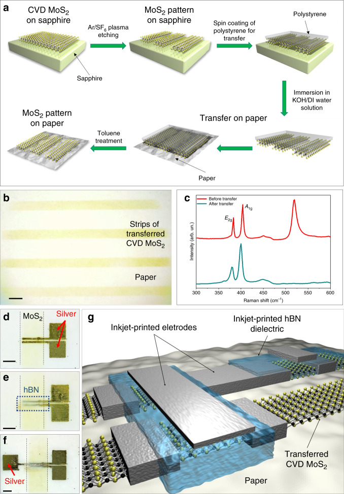
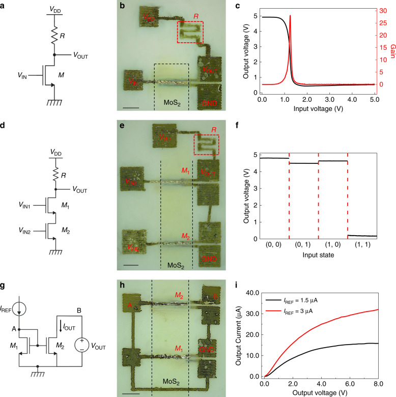
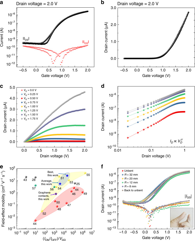
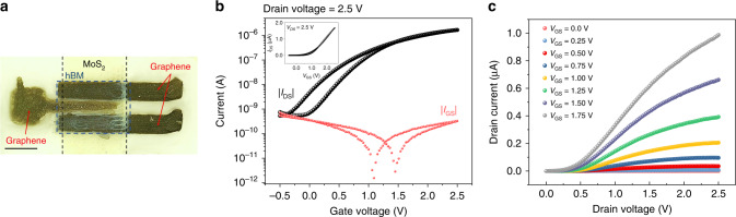
Paper is the ideal substrate for the development of flexible and environmentally sustainable ubiquitous electronic systems, which, combined with two-dimensional materials, could be exploited in many Internet-of-Things applications, ranging from wearable electronics to smart packaging. Here we report high-performance MoS field-effect transistors on paper fabricated with a "channel array" approach, combining the advantages of two large-area techniques: chemical vapor deposition and inkjet-printing. The first allows the pre-deposition of a pattern of MoS; the second, the printing of dielectric layers, contacts, and connections to complete transistors and circuits fabrication. Average I/I of 8 × 10 (up to 5 × 10) and mobility of 5.5 cm V s (up to 26 cm V s) are obtained. Fully functional integrated circuits of digital and analog building blocks, such as logic gates and current mirrors, are demonstrated, highlighting the potential of this approach for ubiquitous electronics on paper.
纸张是开发柔性且环境可持续的普适电子系统的理想基底,该系统与二维材料相结合,可应用于许多物联网应用中,从可穿戴电子设备到智能包装。在此,我们报告了采用“通道阵列”方法在纸张上制备的高性能MoS场效应晶体管,该方法结合了两种大面积技术的优点:化学气相沉积和喷墨打印。第一种技术允许预先沉积MoS图案;第二种技术则用于打印介电层、触点以及连接部分,以完成晶体管和电路的制造。获得了8×10(最高可达5×10)的平均I/I以及5.5 cm² V⁻¹ s⁻¹(最高可达26 cm² V⁻¹ s⁻¹)的迁移率。展示了数字和模拟构建模块的全功能集成电路,如逻辑门和电流镜,突出了这种方法在纸张上实现普适电子器件的潜力。