Abedini Dereshgi Sina, Ghobadi Amir, Hajian Hodjat, Butun Bayram, Ozbay Ekmel
Department of Electrical and Electronics Engineering, Bilkent University, Ankara, 06800, Turkey.
Nanotechnology Research Center (NANOTAM), Bilkent University, Ankara, 06800, Turkey.
Sci Rep. 2017 Nov 1;7(1):14872. doi: 10.1038/s41598-017-13837-8.
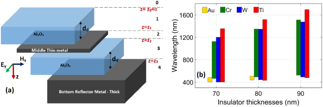
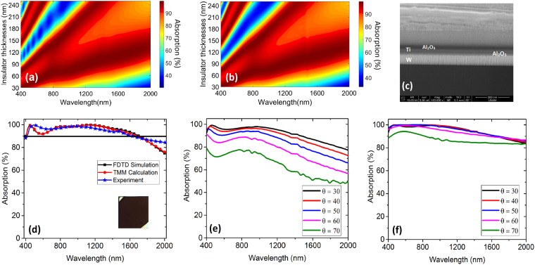
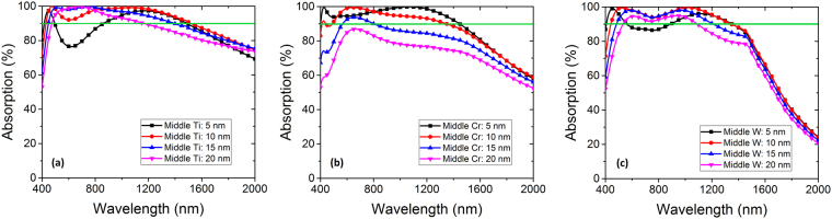
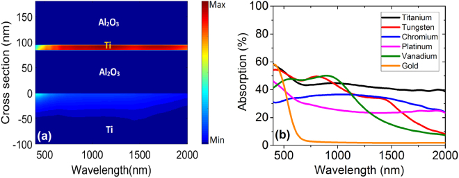
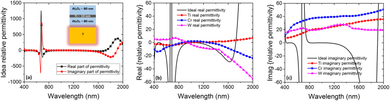
We report ultra-broadband perfect absorbers for visible and near-infrared applications that are based on multilayers of metal-insulator (MI) stacks fabricated employing straightforward layer deposition techniques and are, therefore, lithography-free and large-scale compatible. We scrutinize the impact of different physical parameters of an MIMI absorber structure with analysis of each contributing metal layer. After obtaining the optimal design parameters (i.e. material selection and their thicknesses) with both simulation and numerical analysis (Transfer Matrix Method) methods, an experimental sample is fabricated and characterized. Our fabricated MIMI absorber consists of an optically thick tungsten (W) back reflector layer followed by 80 nm aluminum oxide (AlO), 10 nm titanium (Ti), and finally another 80 nm AlO. The experimental results demonstrate over 90 percent absorption between 400 nm and 1640 nm wavelengths that is optimized for ultra-broadband absorption in MIMI structures. Moreover, the impedance matching method with free-space is used to shed light on the metallic layer selection process.
我们报道了用于可见光和近红外应用的超宽带完美吸收体,该吸收体基于采用直接层沉积技术制造的金属-绝缘体(MI)堆栈多层结构,因此无需光刻且与大规模制造兼容。我们通过分析每个贡献金属层,仔细研究了MIMI吸收体结构不同物理参数的影响。在通过模拟和数值分析(传输矩阵法)方法获得最佳设计参数(即材料选择及其厚度)后,制作并表征了一个实验样品。我们制作的MIMI吸收体由一个光学厚度较大的钨(W)背反射层组成,其后是80纳米的氧化铝(AlO)、10纳米的钛(Ti),最后是另一个80纳米的AlO。实验结果表明,在400纳米至1640纳米波长之间的吸收率超过90%,这是针对MIMI结构中的超宽带吸收进行优化的。此外,采用与自由空间的阻抗匹配方法来阐明金属层的选择过程。