Gilboa Tal, Zrehen Adam, Girsault Arik, Meller Amit
Department of Biomedical Engineering, The Technion - Israel Institute of Technology, Haifa, 32000, Israel.
Sci Rep. 2018 Jun 27;8(1):9765. doi: 10.1038/s41598-018-28136-z.
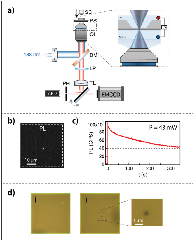
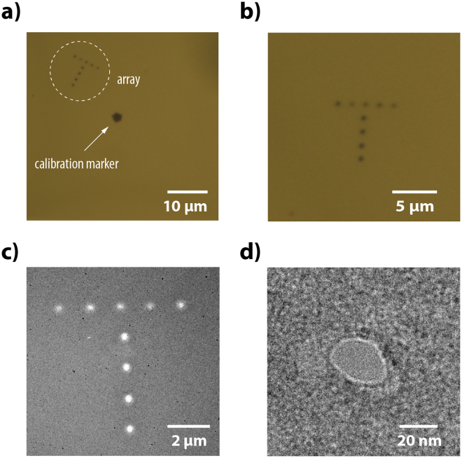
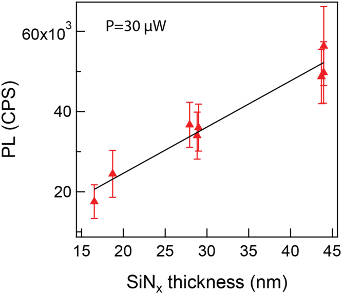
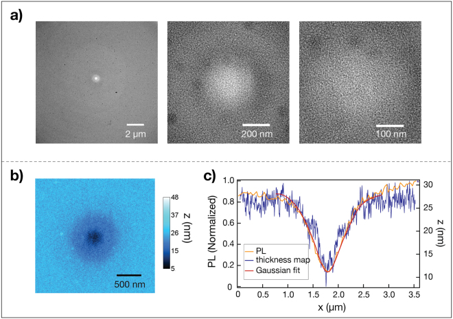
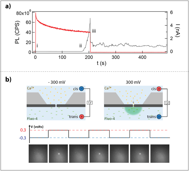
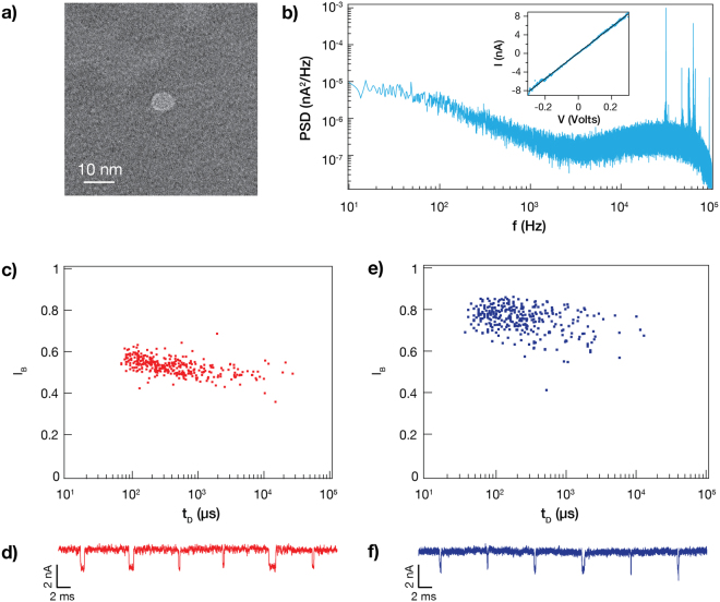
Solid-state nanopores (ssNPs) are extremely versatile single-molecule sensors and their potential have been established in numerous biomedical applications. However, the fabrication of ssNPs remains the main bottleneck to their widespread use. Herein, we introduce a rapid and localizable ssNPs fabrication method based on feedback-controlled optical etching. We show that a focused blue laser beam irreversibly etches silicon nitride (SiN) membranes in solution. Furthermore, photoluminescence (PL) emitted from the SiN is used to monitor the etching process in real-time, hence permitting rate adjustment. Transmission electron microscopy (TEM) images of the etched area reveal an inverted Gaussian thickness profile, corresponding to the intensity point spread function of the laser beam. Continued laser exposure leads to the opening of a nanopore, which can be controlled to reproducibly fabricate nanopores of different sizes. The optically-formed ssNPs exhibit electrical noise on par with TEM-drilled pores, and translocate DNA and proteins readily. Notably, due to the localized thinning, the laser-drilled ssNPs exhibit highly suppressed background PL and improved spatial resolution. Given the total control over the nanopore position, this easily implemented method is ideally suited for electro-optical sensing and opens up the possibility of fabricating large nanopore arrays in situ.
固态纳米孔(ssNPs)是极其通用的单分子传感器,其潜力已在众多生物医学应用中得到证实。然而,ssNPs的制造仍然是其广泛应用的主要瓶颈。在此,我们介绍一种基于反馈控制光学蚀刻的快速且可定位的ssNPs制造方法。我们表明,聚焦的蓝光激光束可在溶液中不可逆地蚀刻氮化硅(SiN)膜。此外,从SiN发射的光致发光(PL)用于实时监测蚀刻过程,从而实现蚀刻速率的调整。蚀刻区域的透射电子显微镜(TEM)图像显示出倒高斯厚度分布,与激光束的强度点扩散函数相对应。持续的激光照射会导致纳米孔的形成,并且可以控制以可重复地制造不同尺寸的纳米孔。光学形成的ssNPs表现出与TEM钻孔孔相当的电噪声,并且能够轻松地使DNA和蛋白质易位。值得注意的是,由于局部变薄,激光钻孔的ssNPs表现出高度抑制的背景PL和提高的空间分辨率。鉴于对纳米孔位置的完全控制,这种易于实施的方法非常适合电光传感,并开辟了原位制造大型纳米孔阵列的可能性。