School of Electrical & Computer Engineering and Birck Nanotechnology Center, Purdue University, West Lafayette, Indiana, 47907, USA.
Geballe Laboratory for Advanced Materials, Stanford University, Stanford, CA, 94305, USA.
Nat Commun. 2018 Jul 10;9(1):2673. doi: 10.1038/s41467-018-05034-6.
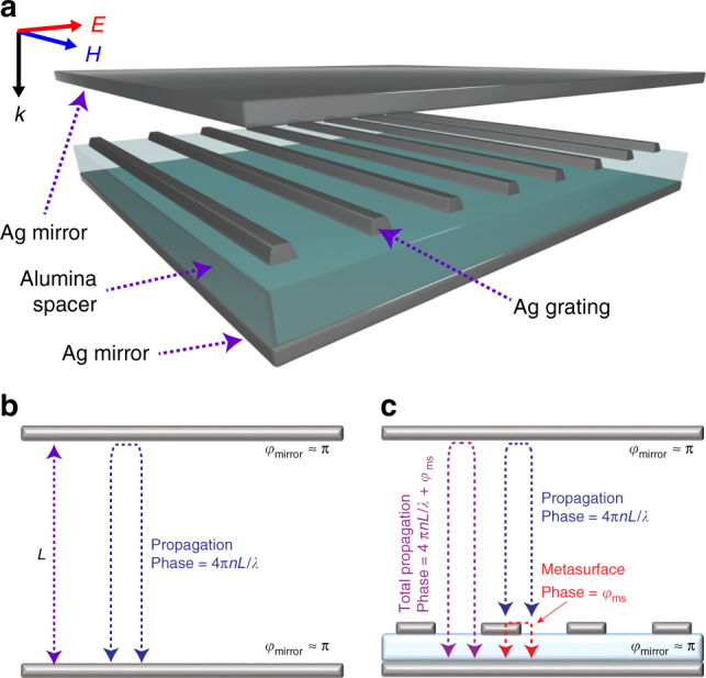
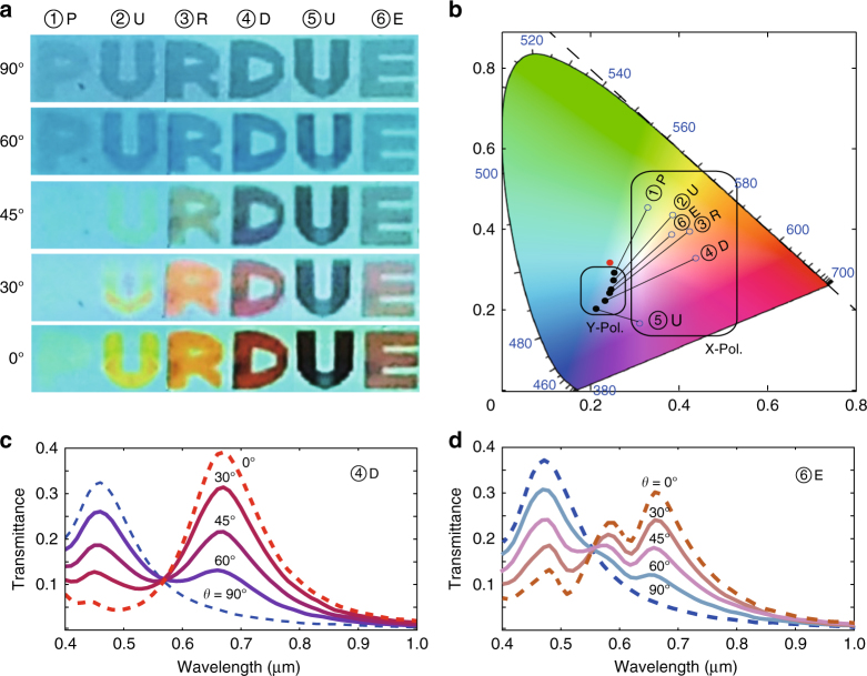
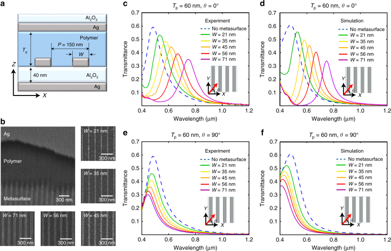
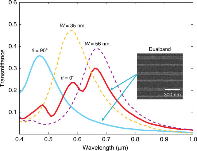
Over the past years, photonic metasurfaces have demonstrated their remarkable and diverse capabilities in advanced control over light propagation. Here, we demonstrate that these artificial films of deeply subwavelength thickness also offer new unparalleled capabilities in decreasing the overall dimensions of integrated optical systems. We propose an original approach of embedding a metasurface inside an optical cavity-one of the most fundamental optical elements-to drastically scale-down its thickness. By modifying the Fabry-Pérot interferometric principle, this methodology is shown to reduce the metasurface-based nanocavity thickness below the conventional λ/(2n) minimum. In addition, the nanocavities with embedded metasurfaces can support independently tunable resonances at multiple bands. As a proof-of-concept, using nanostructured metasurfaces within 100-nm nanocavities, we experimentally demonstrate high spatial resolution colour filtering and spectral imaging. The proposed approach can be extrapolated to compact integrated optical systems on-a-chip such as VCSEL's, high-resolution spatial light modulators, imaging spectroscopy systems, and bio-sensors.
在过去的几年中,光子超表面在先进的光传播控制方面展示了其显著的和多样化的能力。在这里,我们证明了这些亚波长厚度的人工薄膜还提供了新的无与伦比的能力,可以减少集成光学系统的整体尺寸。我们提出了一种将超表面嵌入光学腔中的新方法,这是最基本的光学元件之一,以大幅减小其厚度。通过修改法布里-珀罗干涉原理,该方法被证明可以将基于超表面的纳米腔厚度降低到低于常规的 λ/(2n)最小值。此外,具有嵌入式超表面的纳米腔可以支持在多个波段独立可调谐的共振。作为概念验证,我们使用 100nm 纳米腔中的纳米结构超表面,实验演示了高空间分辨率的颜色滤波和光谱成像。所提出的方法可以扩展到片上的紧凑型集成光学系统,如 VCSEL、高分辨率空间光调制器、成像光谱学系统和生物传感器。