Ji Xianghai, Chen Xiren, Yang Xiaoguang, Zhang Xingwang, Shao Jun, Yang Tao
Key Laboratory of Semiconductor Materials Science, Institute of Semiconductors, Chinese Academy of Sciences, Beijing, 100083, People's Republic of China.
College of Materials Science and Opto-Electronic Technology, University of Chinese Academy of Sciences, Beijing, 100049, People's Republic of China.
Nanoscale Res Lett. 2018 Sep 5;13(1):269. doi: 10.1186/s11671-018-2690-3.
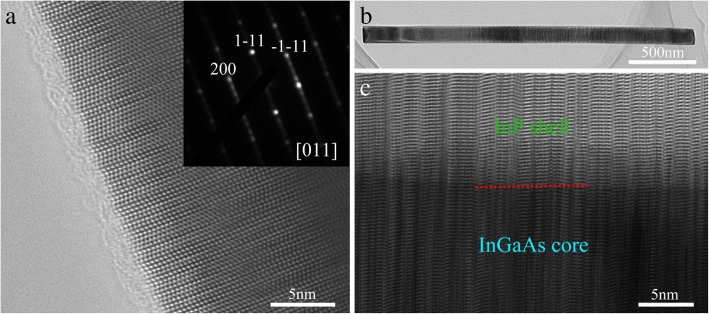
We report on the growth and characterization of InGaAs/InP core-shell nanowires on Si-(111) substrates by metal-organic chemical vapor deposition (MOCVD). The strain at the core-shell interface induced by the large lattice mismatch between the InGaAs core and InP shell materials has strong influence on the growth behavior of the InP shell, leading to the asymmetric growth of InP shell around the InGaAs core and even to the bending of the nanowires. Transmission electron microscopy (TEM) measurements reveal that the InP shell is coherent with the InGaAs core without any misfit dislocations. Furthermore, photoluminescence (PL) measurements at 77 K show that the PL peak intensity from the InGaAs/InP core-shell nanowires displays a ∼ 100 times enhancement compared to the only InGaAs core sample without InP shell due to the passivation of surface states and effective carrier confinement resulting from InP shell layer. The results obtained here further our understanding of the growth behavior of strained core-shell heterostructure nanowires and may open new possibilities for applications in InGaAs/InP heterostructure nanowire-based optoelectronic devices on Si platform.
我们报道了通过金属有机化学气相沉积(MOCVD)在Si-(111)衬底上生长InGaAs/InP核壳纳米线及其特性。InGaAs核与InP壳材料之间较大的晶格失配在核壳界面处引起的应变,对InP壳的生长行为有强烈影响,导致InP壳在InGaAs核周围不对称生长,甚至使纳米线弯曲。透射电子显微镜(TEM)测量表明,InP壳与InGaAs核是相干的,没有任何失配位错。此外,77 K下的光致发光(PL)测量表明,与没有InP壳的纯InGaAs核样品相比,InGaAs/InP核壳纳米线的PL峰强度提高了约100倍,这归因于表面态的钝化以及InP壳层导致的有效载流子限制。此处获得的结果进一步加深了我们对应变核壳异质结构纳米线生长行为的理解,并可能为基于InGaAs/InP异质结构纳米线的Si平台光电器件的应用开辟新的可能性。