• 文献检索
  • 文档翻译
  • 深度研究
  • 学术资讯
  • Suppr Zotero 插件Zotero 插件
  • 邀请有礼
  • 套餐&价格
  • 历史记录
应用&插件
Suppr Zotero 插件Zotero 插件浏览器插件Mac 客户端Windows 客户端微信小程序
定价
高级版会员购买积分包购买API积分包
服务
文献检索文档翻译深度研究API 文档MCP 服务
关于我们
关于 Suppr公司介绍联系我们用户协议隐私条款
关注我们

Suppr 超能文献

核心技术专利:CN118964589B侵权必究
粤ICP备2023148730 号-1Suppr @ 2026

文献检索

告别复杂PubMed语法,用中文像聊天一样搜索,搜遍4000万医学文献。AI智能推荐,让科研检索更轻松。

立即免费搜索

文件翻译

保留排版,准确专业,支持PDF/Word/PPT等文件格式,支持 12+语言互译。

免费翻译文档

深度研究

AI帮你快速写综述,25分钟生成高质量综述,智能提取关键信息,辅助科研写作。

立即免费体验

嵌入等离子体波导中的纳米金刚石中单个锗空位的片上激发

On-chip excitation of single germanium vacancies in nanodiamonds embedded in plasmonic waveguides.

作者信息

Siampour Hamidreza, Kumar Shailesh, Davydov Valery A, Kulikova Liudmila F, Agafonov Viatcheslav N, Bozhevolnyi Sergey I

机构信息

1Centre for Nano Optics, University of Southern Denmark, Campusvej 55, Odense M, DK-5230 Denmark.

2L.F. Vereshchagin Institute for High Pressure Physics, Russian Academy of Sciences, Troitsk, Moscow, 142190 Russia.

出版信息

Light Sci Appl. 2018 Sep 12;7:61. doi: 10.1038/s41377-018-0062-5. eCollection 2018.

DOI:10.1038/s41377-018-0062-5
PMID:30245809
原文链接:https://pmc.ncbi.nlm.nih.gov/articles/PMC6134053/
Abstract

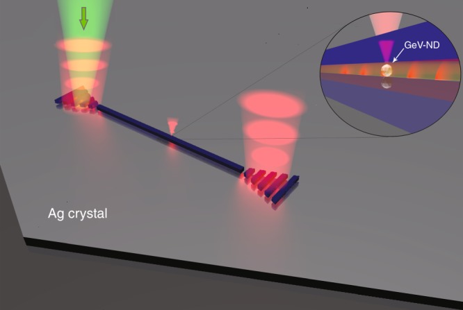
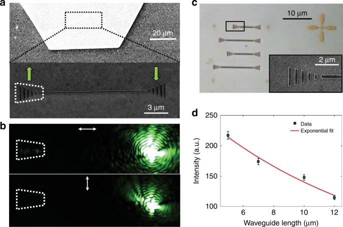
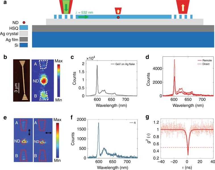
Monolithic integration of quantum emitters in nanoscale plasmonic circuitry requires low-loss plasmonic configurations capable of confining light well below the diffraction limit. We demonstrated on-chip remote excitation of nanodiamond-embedded single quantum emitters by plasmonic modes of dielectric ridges atop colloidal silver crystals. The nanodiamonds were produced to incorporate single germanium-vacancy (GeV) centres, providing bright, spectrally narrow and stable single-photon sources suitable for highly integrated circuits. Using electron-beam lithography with hydrogen silsesquioxane (HSQ) resist, dielectric-loaded surface plasmon polariton waveguides (DLSPPWs) were fabricated on single crystalline silver plates to contain those of deposited nanodiamonds that are found to feature appropriate single GeV centres. The low-loss plasmonic configuration enabled the 532-nm pump laser light to propagate on-chip in the DLSPPW and reach to an embedded nanodiamond where a single GeV centre was incorporated. The remote GeV emitter was thereby excited and coupled to spatially confined DLSPPW modes with an outstanding figure-of-merit of 180 due to a ~six-fold Purcell enhancement, ~56% coupling efficiency and ~33 μm transmission length, thereby opening new avenues for the implementation of nanoscale functional quantum devices.

摘要

将量子发射器单片集成到纳米级等离子体电路中,需要低损耗的等离子体结构,能够将光限制在远低于衍射极限的范围内。我们通过胶体银晶体顶部介电脊的等离子体模式,展示了对嵌入纳米金刚石的单量子发射器进行片上远程激发。制备的纳米金刚石包含单个锗空位(GeV)中心,提供了适用于高度集成电路的明亮、光谱窄且稳定的单光子源。使用电子束光刻技术和氢倍半硅氧烷(HSQ)抗蚀剂,在单晶银板上制造了加载电介质的表面等离子体激元极化子波导(DLSPPW),以容纳那些含有合适单GeV中心的沉积纳米金刚石。这种低损耗等离子体结构使532纳米泵浦激光能够在DLSPPW中在片上传播,并到达嵌入了单个GeV中心的纳米金刚石。由于约六倍的珀塞尔增强、约56% 的耦合效率和约33微米 的传输长度,远程GeV发射器因此被激发并耦合到空间受限的DLSPPW模式,其品质因数高达180,从而为实现纳米级功能量子器件开辟了新途径。

https://cdn.ncbi.nlm.nih.gov/pmc/blobs/a69b/6134053/f1bcdfc6a5d0/41377_2018_62_Fig6_HTML.jpg
https://cdn.ncbi.nlm.nih.gov/pmc/blobs/a69b/6134053/972820302069/41377_2018_62_Fig1_HTML.jpg
https://cdn.ncbi.nlm.nih.gov/pmc/blobs/a69b/6134053/c4a49dbd21fa/41377_2018_62_Fig2_HTML.jpg
https://cdn.ncbi.nlm.nih.gov/pmc/blobs/a69b/6134053/23a0262a49cd/41377_2018_62_Fig3_HTML.jpg
https://cdn.ncbi.nlm.nih.gov/pmc/blobs/a69b/6134053/6f804250fb6d/41377_2018_62_Fig4_HTML.jpg
https://cdn.ncbi.nlm.nih.gov/pmc/blobs/a69b/6134053/341d6d78b1f6/41377_2018_62_Fig5_HTML.jpg
https://cdn.ncbi.nlm.nih.gov/pmc/blobs/a69b/6134053/f1bcdfc6a5d0/41377_2018_62_Fig6_HTML.jpg

相似文献

1
On-chip excitation of single germanium vacancies in nanodiamonds embedded in plasmonic waveguides.嵌入等离子体波导中的纳米金刚石中单个锗空位的片上激发
Light Sci Appl. 2018 Sep 12;7:61. doi: 10.1038/s41377-018-0062-5. eCollection 2018.
2
Chip-integrated plasmonic cavity-enhanced single nitrogen-vacancy center emission.片上集成等离子体腔增强单氮空位中心辐射。
Nanoscale. 2017 Nov 23;9(45):17902-17908. doi: 10.1039/c7nr05675c.
3
Fluorescence enhancement of a single germanium vacancy center in a nanodiamond by a plasmonic Bragg cavity.通过等离子体布拉格腔增强纳米金刚石中单个锗空位中心的荧光
J Chem Phys. 2021 Jan 28;154(4):044303. doi: 10.1063/5.0033507.
4
On-chip detection of radiation guided by dielectric-loaded plasmonic waveguides.基于介质加载等离子体导波的片上辐射检测。
Nano Lett. 2015 Jan 14;15(1):476-80. doi: 10.1021/nl5037885. Epub 2014 Dec 8.
5
Efficient interfacing photonic and long-range dielectric-loaded plasmonic waveguides.高效连接光子和长程介质加载等离子体波导。
Opt Express. 2015 Apr 6;23(7):9100-8. doi: 10.1364/OE.23.009100.
6
Fiber-coupled dielectric-loaded plasmonic waveguides.光纤耦合介质加载等离子体波导。
Opt Express. 2010 Mar 1;18(5):5314-9. doi: 10.1364/OE.18.005314.
7
A Single-Crystalline Silver Plasmonic Circuit for Visible Quantum Emitters.用于可见量子发射器的单晶硅银等离子体电路。
Nano Lett. 2019 May 8;19(5):3238-3243. doi: 10.1021/acs.nanolett.9b00773. Epub 2019 Apr 26.
8
Optomagnetic plasmonic nanocircuits.光磁等离子体纳米电路
Nanoscale Adv. 2019 Jun 25;1(8):3131-3138. doi: 10.1039/c9na00351g. eCollection 2019 Aug 6.
9
Power monitoring in dielectric-loaded plasmonic waveguides with internal Wheatstone bridges.基于内部惠斯通电桥的介质加载等离子体波导中的功率监测。
Opt Express. 2013 Mar 11;21(5):5300-8. doi: 10.1364/OE.21.005300.
10
Enhanced Plasmonic Trapping and Fluorescent Emission of Nitrogen-Vacancy Nanodiamonds Using a High-Efficiency Nanofocusing Device.使用高效纳米聚焦装置增强氮空位纳米金刚石的表面等离子体捕获和荧光发射
Nano Lett. 2024 Sep 18;24(37):11661-11668. doi: 10.1021/acs.nanolett.4c03163. Epub 2024 Sep 9.

引用本文的文献

1
Strongly coupled spins of silicon-vacancy centers inside a nanodiamond with sub-megahertz linewidth.具有亚兆赫兹线宽的纳米金刚石内部硅空位中心的强耦合自旋。
Nanophotonics. 2024 Mar 13;13(13):2361-2366. doi: 10.1515/nanoph-2023-0927. eCollection 2024 May.
2
Directional Coupling to a λ/5000 Nanowaveguide.与λ/5000纳米波导的定向耦合
ACS Nano. 2024 Nov 5;18(44):30626-30637. doi: 10.1021/acsnano.4c09434. Epub 2024 Oct 21.
3
Enhanced Plasmonic Trapping and Fluorescent Emission of Nitrogen-Vacancy Nanodiamonds Using a High-Efficiency Nanofocusing Device.

本文引用的文献

1
Efficient photon coupling from a diamond nitrogen vacancy center by integration with silica fiber.通过与石英光纤集成实现从金刚石氮空位中心的高效光子耦合。
Light Sci Appl. 2016 Feb 12;5(2):e16032. doi: 10.1038/lsa.2016.32. eCollection 2016 Feb.
2
Tin-Vacancy Quantum Emitters in Diamond.金刚石中的锡空位量子发射器
Phys Rev Lett. 2017 Dec 22;119(25):253601. doi: 10.1103/PhysRevLett.119.253601.
3
Chip-integrated plasmonic cavity-enhanced single nitrogen-vacancy center emission.片上集成等离子体腔增强单氮空位中心辐射。
使用高效纳米聚焦装置增强氮空位纳米金刚石的表面等离子体捕获和荧光发射
Nano Lett. 2024 Sep 18;24(37):11661-11668. doi: 10.1021/acs.nanolett.4c03163. Epub 2024 Sep 9.
4
Engineering the Outcoupling Pathways in Plasmonic Tunnel Junctions via Photonic Mode Dispersion for Low-Loss Waveguiding.通过光子模式色散设计等离子体隧道结中的出射耦合路径以实现低损耗波导
ACS Nano. 2024 Jan 9;18(1):1149-1156. doi: 10.1021/acsnano.3c10832. Epub 2023 Dec 26.
5
Multiple channelling single-photon emission with scattering holography designed metasurfaces.基于散射全息设计超表面实现多通道单光子发射
Nat Commun. 2023 Oct 6;14(1):6253. doi: 10.1038/s41467-023-42046-3.
6
Light-Responsive Supramolecular Nanotubes-Based Chiral Plasmonic Assemblies.基于光响应超分子纳米管的手性等离子体组装体。
ACS Nano. 2023 Mar 28;17(6):5548-5560. doi: 10.1021/acsnano.2c10955. Epub 2023 Mar 10.
7
Optomagnetic plasmonic nanocircuits.光磁等离子体纳米电路
Nanoscale Adv. 2019 Jun 25;1(8):3131-3138. doi: 10.1039/c9na00351g. eCollection 2019 Aug 6.
8
Duo Emission of CVD Nanodiamonds Doped by SiV and GeV Color Centers: Effects of Growth Conditions.硅空位(SiV)和锗空位(GeV)色心掺杂的化学气相沉积纳米金刚石的双发射:生长条件的影响
Materials (Basel). 2022 May 18;15(10):3589. doi: 10.3390/ma15103589.
9
Room-temperature single-photon emitters in silicon nitride.氮化硅中的室温单光子发射器
Sci Adv. 2021 Dec 10;7(50):eabj0627. doi: 10.1126/sciadv.abj0627.
10
Intracellular Thermal Probing Using Aggregated Fluorescent Nanodiamonds.利用聚集荧光纳米金刚石进行细胞内热探测。
Adv Sci (Weinh). 2022 Jan;9(3):e2103354. doi: 10.1002/advs.202103354. Epub 2021 Nov 23.
Nanoscale. 2017 Nov 23;9(45):17902-17908. doi: 10.1039/c7nr05675c.
4
Electrically driven monolithic subwavelength plasmonic interconnect circuits.电驱动单片亚波长等离子体互连电路。
Sci Adv. 2017 Oct 20;3(10):e1701456. doi: 10.1126/sciadv.1701456. eCollection 2017 Oct.
5
Improved emission of SiV diamond color centers embedded into concave plasmonic core-shell nanoresonators.嵌入凹面等离激元核壳纳米谐振器中的硅空位金刚石色心的发射增强。
Sci Rep. 2017 Oct 23;7(1):13845. doi: 10.1038/s41598-017-14227-w.
6
Chip-Based All-Optical Control of Single Molecules Coherently Coupled to a Nanoguide.基于芯片的全光学控制单个分子与纳米导相干耦合。
Nano Lett. 2017 Aug 9;17(8):4941-4945. doi: 10.1021/acs.nanolett.7b02033. Epub 2017 Jul 10.
7
Quantum Nonlinear Optics with a Germanium-Vacancy Color Center in a Nanoscale Diamond Waveguide.纳米级金刚石波导中锗空位色心的量子非线性光学
Phys Rev Lett. 2017 Jun 2;118(22):223603. doi: 10.1103/PhysRevLett.118.223603. Epub 2017 May 31.
8
Ultrabright Linearly Polarized Photon Generation from a Nitrogen Vacancy Center in a Nanocube Dimer Antenna.从纳米立方体二聚体天线中的氮空位中心产生超亮线偏振光子。
Nano Lett. 2017 Jun 14;17(6):3889-3895. doi: 10.1021/acs.nanolett.7b01436. Epub 2017 May 8.
9
Plasmonic Waveguide-Integrated Nanowire Laser.等离子体波导集成纳米线激光器
Nano Lett. 2017 Feb 8;17(2):747-754. doi: 10.1021/acs.nanolett.6b03879. Epub 2017 Jan 9.
10
High-yield fabrication and properties of 1.4 nm nanodiamonds with narrow size distribution.高产制备和窄分布尺寸 1.4nm 纳米金刚石的性能。
Sci Rep. 2016 Dec 2;6:38419. doi: 10.1038/srep38419.