• 文献检索
  • 文档翻译
  • 深度研究
  • 学术资讯
  • Suppr Zotero 插件Zotero 插件
  • 邀请有礼
  • 套餐&价格
  • 历史记录
应用&插件
Suppr Zotero 插件Zotero 插件浏览器插件Mac 客户端Windows 客户端微信小程序
定价
高级版会员购买积分包购买API积分包
服务
文献检索文档翻译深度研究API 文档MCP 服务
关于我们
关于 Suppr公司介绍联系我们用户协议隐私条款
关注我们

Suppr 超能文献

核心技术专利:CN118964589B侵权必究
粤ICP备2023148730 号-1Suppr @ 2026

文献检索

告别复杂PubMed语法,用中文像聊天一样搜索,搜遍4000万医学文献。AI智能推荐,让科研检索更轻松。

立即免费搜索

文件翻译

保留排版,准确专业,支持PDF/Word/PPT等文件格式,支持 12+语言互译。

免费翻译文档

深度研究

AI帮你快速写综述,25分钟生成高质量综述,智能提取关键信息,辅助科研写作。

立即免费体验

锗掺杂垂直氮化镓肖特基势垒二极管的恢复性能

Recovery Performance of Ge-Doped Vertical GaN Schottky Barrier Diodes.

作者信息

Gu Hong, Tian Feifei, Zhang Chunyu, Xu Ke, Wang Jiale, Chen Yong, Deng Xuanhua, Liu Xinke

机构信息

College of Materials Science and Engineering, Guangdong Research Center for Interfacial Engineering of Functional Materials, Shenzhen Key Laboratory of Special Functional Materials, Chinese Engineering and Research Institute of Microelectronics, Shenzhen University, Shenzhen, 518060, People's Republic of China.

Key Laboratory of Optoelectronic Devices and Systems of Ministry of Education and Guangdong Province, College of Optoelectronic Engineering, Shenzhen University, Shenzhen, 518060, People's Republic of China.

出版信息

Nanoscale Res Lett. 2019 Jan 31;14(1):40. doi: 10.1186/s11671-019-2872-7.

DOI:10.1186/s11671-019-2872-7
PMID:30706287
原文链接:https://pmc.ncbi.nlm.nih.gov/articles/PMC6355890/
Abstract

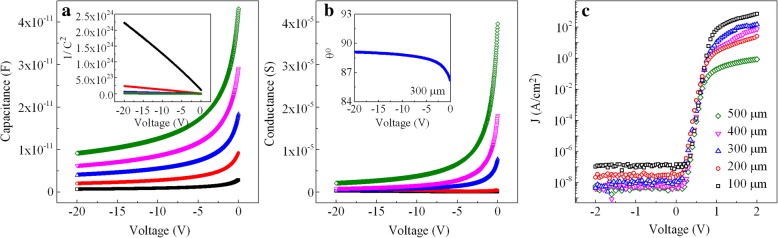
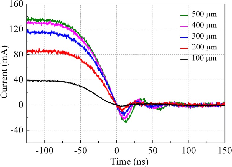
Vertical GaN Schottky barrier diodes (SBDs) were fabricated on Ge-doped free-standing GaN substrates. The crystal quality of the SBDs was characterized by cathode luminescence measurement, and the dislocation density was determined to be ~ 1.3 × 10 cm. With the electrical performance measurements conducted, the SBDs show a low turn-on voltage V (0.700.78 V) and high current I/I ratio (9.9 × 101.3 × 10). The reverse recovery characteristics were investigated. The reverse recovery time was obtained to be 15.8, 16.2, 18.1, 21.22, and 24.5 ns for the 100-, 200-, 300-, 400-, and 500-μm-diameter SBDs, respectively. Meanwhile, the reverse recovery time and reverse recovery charge both show a significant positive correlation with the electrode area.

摘要

垂直氮化镓肖特基势垒二极管(SBD)是在掺锗的自支撑氮化镓衬底上制备的。通过阴极发光测量对SBD的晶体质量进行了表征,确定位错密度约为1.3×10¹⁰cm⁻²。通过电学性能测量,SBD显示出低开启电压V(0.700.78V)和高电流I/I比(9.9×10⁷1.3×10⁸)。研究了反向恢复特性。对于直径为100、200、300、400和500μm的SBD,反向恢复时间分别为15.8、16.2、18.1、21.22和24.5ns。同时,反向恢复时间和反向恢复电荷均与电极面积呈显著正相关。

https://cdn.ncbi.nlm.nih.gov/pmc/blobs/6f4c/6355890/fe5f3337e2b8/11671_2019_2872_Fig7_HTML.jpg
https://cdn.ncbi.nlm.nih.gov/pmc/blobs/6f4c/6355890/8ce1aa3928ad/11671_2019_2872_Fig1_HTML.jpg
https://cdn.ncbi.nlm.nih.gov/pmc/blobs/6f4c/6355890/2e214157bbdd/11671_2019_2872_Fig2_HTML.jpg
https://cdn.ncbi.nlm.nih.gov/pmc/blobs/6f4c/6355890/7bb27dc4b283/11671_2019_2872_Fig3_HTML.jpg
https://cdn.ncbi.nlm.nih.gov/pmc/blobs/6f4c/6355890/b3065ef4377d/11671_2019_2872_Fig4_HTML.jpg
https://cdn.ncbi.nlm.nih.gov/pmc/blobs/6f4c/6355890/3cbca28be824/11671_2019_2872_Fig5_HTML.jpg
https://cdn.ncbi.nlm.nih.gov/pmc/blobs/6f4c/6355890/10ebe59d4206/11671_2019_2872_Fig6_HTML.jpg
https://cdn.ncbi.nlm.nih.gov/pmc/blobs/6f4c/6355890/fe5f3337e2b8/11671_2019_2872_Fig7_HTML.jpg

相似文献

1
Recovery Performance of Ge-Doped Vertical GaN Schottky Barrier Diodes.锗掺杂垂直氮化镓肖特基势垒二极管的恢复性能
Nanoscale Res Lett. 2019 Jan 31;14(1):40. doi: 10.1186/s11671-019-2872-7.
2
Vertical GaN-on-GaN Schottky Diodes as α-Particle Radiation Sensors.垂直氮化镓基肖特基二极管作为α粒子辐射传感器。
Micromachines (Basel). 2020 May 20;11(5):519. doi: 10.3390/mi11050519.
3
Low Voltage High-Energy α-Particle Detectors by GaN-on-GaN Schottky Diodes with Record-High Charge Collection Efficiency.氮化镓肖特基二极管的低压高能 α 粒子探测器,具有创纪录的高电荷收集效率。
Sensors (Basel). 2019 Nov 21;19(23):5107. doi: 10.3390/s19235107.
4
Development and Modelling of Gallium Nitride Based Lateral Schottky Barrier Diodes with Anode Recesses for mmWave and THz Applications.用于毫米波和太赫兹应用的具有阳极凹槽的氮化镓基横向肖特基势垒二极管的开发与建模
Micromachines (Basel). 2022 Dec 20;14(1):2. doi: 10.3390/mi14010002.
5
Theoretical and Experimental Study on AlGaN/GaN Schottky Barrier Diode on Si Substrate with Double-Heterojunction.基于硅衬底的具有双异质结的氮化铝镓/氮化镓肖特基势垒二极管的理论与实验研究
Nanoscale Res Lett. 2020 Jul 16;15(1):149. doi: 10.1186/s11671-020-03376-z.
6
Thermal Behavior of an AlGaN/GaN-Based Schottky Barrier Diode on Diamond and Silicon Substrates.基于AlGaN/GaN的肖特基势垒二极管在金刚石和硅衬底上的热行为
J Nanosci Nanotechnol. 2021 Aug 1;21(8):4429-4433. doi: 10.1166/jnn.2021.19421.
7
Electronic Transport Mechanism for Schottky Diodes Formed by Au/HVPE a-Plane GaN Templates Grown via In Situ GaN Nanodot Formation.通过原位形成GaN纳米点生长的Au/HVPE a面GaN模板形成的肖特基二极管的电子传输机制
Nanomaterials (Basel). 2018 Jun 2;8(6):397. doi: 10.3390/nano8060397.
8
Solid-State Carbon-Doped GaN Schottky Diodes by Controlling Dissociation of the Graphene Interlayer with a Sputtered AlN Capping Layer.采用溅射 AlN 盖帽层控制石墨烯层的离解制备固态掺碳 GaN 肖特基二极管。
ACS Appl Mater Interfaces. 2019 Dec 26;11(51):48086-48094. doi: 10.1021/acsami.9b18976. Epub 2019 Dec 11.
9
AlGaN/GaN on SiC Devices without a GaN Buffer Layer: Electrical and Noise Characteristics.碳化硅衬底上无氮化镓缓冲层的氮化铝镓/氮化镓器件:电学和噪声特性
Micromachines (Basel). 2020 Dec 20;11(12):1131. doi: 10.3390/mi11121131.
10
Current Transport Mechanism in Palladium Schottky Contact on Si-Based Freestanding GaN.硅基独立式氮化镓上钯肖特基接触中的电流传输机制
Nanomaterials (Basel). 2020 Feb 10;10(2):297. doi: 10.3390/nano10020297.

引用本文的文献

1
Power Electronics Revolutionized: A Comprehensive Analysis of Emerging Wide and Ultrawide Bandgap Devices.电力电子学的变革:对新兴宽禁带和超宽禁带器件的全面分析。
Micromachines (Basel). 2023 Oct 31;14(11):2045. doi: 10.3390/mi14112045.
2
Review of Recent Progress on Vertical GaN-Based PN Diodes.基于垂直氮化镓的PN二极管的近期进展综述。
Nanoscale Res Lett. 2021 Jun 7;16(1):101. doi: 10.1186/s11671-021-03554-7.
3
Strain and Electric Field Controllable Schottky Barriers and Contact Types in Graphene-MoTe van der Waals Heterostructure.

本文引用的文献

1
On the p-AlGaN/n-AlGaN/p-AlGaN Current Spreading Layer for AlGaN-based Deep Ultraviolet Light-Emitting Diodes.用于基于AlGaN的深紫外发光二极管的p-AlGaN/n-AlGaN/p-AlGaN电流扩展层
Nanoscale Res Lett. 2018 Nov 8;13(1):355. doi: 10.1186/s11671-018-2776-y.
2
Thickness Dependence on Interfacial and Electrical Properties in Atomic Layer Deposited AlN on c-plane GaN.原子层沉积在c面氮化镓上的氮化铝中厚度对界面和电学性质的依赖性
Nanoscale Res Lett. 2018 Aug 10;13(1):232. doi: 10.1186/s11671-018-2645-8.
3
Effect of doping on the intersubband absorption in Si- and Ge-doped GaN/AlN heterostructures.
石墨烯 - 碲化钼范德华异质结构中应变和电场可控的肖特基势垒及接触类型
Nanoscale Res Lett. 2020 Sep 21;15(1):180. doi: 10.1186/s11671-020-03409-7.
掺杂对 Si 和 Ge 掺杂 GaN/AlN 异质结构中子带吸收的影响。
Nanotechnology. 2017 Oct 6;28(40):405204. doi: 10.1088/1361-6528/aa8504. Epub 2017 Aug 8.