Paul Scherrer Institut, 5232 Villigen PSI, Switzerland.
DECTRIS Ltd, 5405 Baden-Daettwil, Switzerland.
Acta Crystallogr D Struct Biol. 2019 May 1;75(Pt 5):458-466. doi: 10.1107/S2059798319003942. Epub 2019 Apr 8.
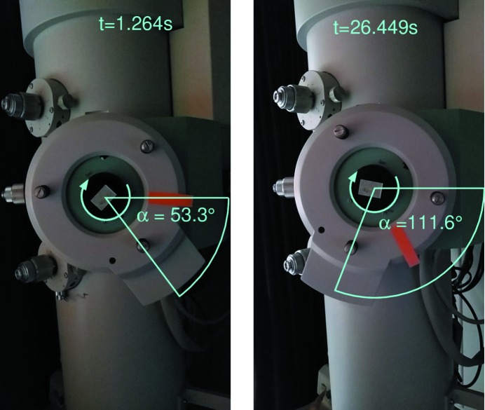
3D electron diffraction has reached a stage where the structures of chemical compounds can be solved productively. Instrumentation is lagging behind this development, and to date dedicated electron diffractometers for data collection based on the rotation method do not exist. Current studies use transmission electron microscopes as a workaround. These are optimized for imaging, which is not optimal for diffraction studies. The beam intensity is very high, it is difficult to create parallel beam illumination and the detectors used for imaging are of only limited use for diffraction studies. In this work, the combination of an EIGER hybrid pixel detector with a transmission electron microscope to construct a productive electron diffractometer is described. The construction not only refers to the combination of hardware but also to the calibration of the system, so that it provides rapid access to the experimental parameters that are necessary for processing diffraction data. Until fully integrated electron diffractometers become available, this describes a setup for productive and efficient operation in chemical crystallography.
3D 电子衍射已经达到了可以有效地解析化合物结构的阶段。仪器设备的发展滞后于这一进展,到目前为止,还没有专门用于基于旋转法采集数据的电子衍射仪。目前的研究使用透射电子显微镜作为一种解决方法。这些显微镜针对成像进行了优化,而不是针对衍射研究进行优化。光束强度非常高,很难创建平行光束照明,并且用于成像的探测器对于衍射研究的用途也非常有限。在这项工作中,描述了将 EIGER 混合像素探测器与透射电子显微镜相结合,构建高效电子衍射仪的方法。该结构不仅涉及硬件的组合,还涉及系统的校准,以便能够快速获得处理衍射数据所需的实验参数。在完全集成的电子衍射仪问世之前,这描述了一种在化学晶体学中进行高效、实用操作的设置。