• 文献检索
  • 文档翻译
  • 深度研究
  • 学术资讯
  • Suppr Zotero 插件Zotero 插件
  • 邀请有礼
  • 套餐&价格
  • 历史记录
应用&插件
Suppr Zotero 插件Zotero 插件浏览器插件Mac 客户端Windows 客户端微信小程序
定价
高级版会员购买积分包购买API积分包
服务
文献检索文档翻译深度研究API 文档MCP 服务
关于我们
关于 Suppr公司介绍联系我们用户协议隐私条款
关注我们

Suppr 超能文献

核心技术专利:CN118964589B侵权必究
粤ICP备2023148730 号-1Suppr @ 2026

文献检索

告别复杂PubMed语法,用中文像聊天一样搜索,搜遍4000万医学文献。AI智能推荐,让科研检索更轻松。

立即免费搜索

文件翻译

保留排版,准确专业,支持PDF/Word/PPT等文件格式,支持 12+语言互译。

免费翻译文档

深度研究

AI帮你快速写综述,25分钟生成高质量综述,智能提取关键信息,辅助科研写作。

立即免费体验

用于钝化接触式 c-Si 太阳能电池的高迁移率氢化氟掺杂氧化铟薄膜。

High-Mobility Hydrogenated Fluorine-Doped Indium Oxide Film for Passivating Contacts c-Si Solar Cells.

机构信息

Photovoltaic Materials and Devices Group , Delft University of Technology , 2628 CD Delft , The Netherlands.

Institute of Photoelectronic Thin Film Devices and Technology of Nankai University , Tianjin 300350 , China.

出版信息

ACS Appl Mater Interfaces. 2019 Dec 11;11(49):45586-45595. doi: 10.1021/acsami.9b14709. Epub 2019 Nov 22.

DOI:10.1021/acsami.9b14709
PMID:31756085
原文链接:https://pmc.ncbi.nlm.nih.gov/articles/PMC6909235/
Abstract

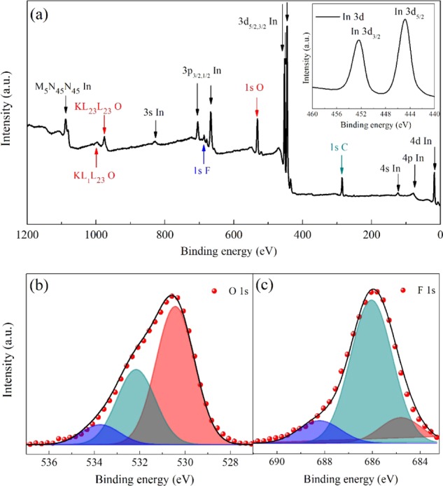
Broadband transparent conductive oxide layers with high electron mobility () are essential to further enhance crystalline silicon (c-Si) solar cell performances. Although metallic cation-doped InO thin films with high (>60 cm V s) have been extensively investigated, the research regarding anion doping is still under development. In particular, fluorine-doped indium oxide (IFO) shows promising optoelectrical properties; however, they have not been tested on c-Si solar cells with passivating contacts. Here, we investigate the properties of hydrogenated IFO (IFO:H) films processed at low substrate temperature and power density by varying the water vapor pressure during deposition. The optimized IFO:H shows a remarkably high of 87 cm V s, a carrier density of 1.2 × 10 cm, and resistivity of 6.2 × 10 Ω cm. Then, we analyzed the compositional, structural, and optoelectrical properties of the optimal IFO:H film. The high quality of the layer was confirmed by the low Urbach energy of 197 meV, compared to 444 meV obtained on the reference indium tin oxide. We implemented IFO:H into different front/back-contacted solar cells with passivating contacts processed at high and low temperatures, obtaining a significant short-circuit current gain of 1.53 mA cm. The best solar cell shows a conversion efficiency of 21.1%.

摘要

宽带透明导电氧化物层具有高电子迁移率(),对于进一步提高晶体硅(c-Si)太阳能电池的性能至关重要。尽管已经广泛研究了具有高(>60 cm V s)的金属阳离子掺杂氧化铟薄膜,但阴离子掺杂的研究仍在发展中。特别是,掺氟氧化铟(IFO)表现出有前景的光电性能;然而,它们尚未在具有钝化接触的 c-Si 太阳能电池上进行测试。在这里,我们研究了通过在沉积过程中改变水蒸气压力在低温和低功率密度下处理的氢化 IFO(IFO:H)薄膜的性质。优化后的 IFO:H 表现出非常高的 87 cm V s、载流子密度为 1.2×10 cm 和电阻率为 6.2×10 Ω cm。然后,我们分析了最佳 IFO:H 薄膜的组成、结构和光电性能。与在参考氧化铟锡上获得的 444 meV 相比,层的低 Urbach 能 197 meV 证实了其高质量。我们将 IFO:H 应用于具有高温和低温处理的钝化接触的不同前/后接触太阳能电池中,获得了 1.53 mA cm 的显著短路电流增益。最佳太阳能电池的转换效率为 21.1%。

https://cdn.ncbi.nlm.nih.gov/pmc/blobs/2466/6909235/1bf8f1ee0fb4/am9b14709_0003.jpg
https://cdn.ncbi.nlm.nih.gov/pmc/blobs/2466/6909235/653430281fec/am9b14709_0005.jpg
https://cdn.ncbi.nlm.nih.gov/pmc/blobs/2466/6909235/57bac2cc0629/am9b14709_0009.jpg
https://cdn.ncbi.nlm.nih.gov/pmc/blobs/2466/6909235/14ef2651e880/am9b14709_0006.jpg
https://cdn.ncbi.nlm.nih.gov/pmc/blobs/2466/6909235/173a346c6c76/am9b14709_0001.jpg
https://cdn.ncbi.nlm.nih.gov/pmc/blobs/2466/6909235/4302be12b3d8/am9b14709_0002.jpg
https://cdn.ncbi.nlm.nih.gov/pmc/blobs/2466/6909235/65c63a71d98f/am9b14709_0007.jpg
https://cdn.ncbi.nlm.nih.gov/pmc/blobs/2466/6909235/97a7888c2d8d/am9b14709_0008.jpg
https://cdn.ncbi.nlm.nih.gov/pmc/blobs/2466/6909235/1bf8f1ee0fb4/am9b14709_0003.jpg

相似文献

1
High-Mobility Hydrogenated Fluorine-Doped Indium Oxide Film for Passivating Contacts c-Si Solar Cells.用于钝化接触式 c-Si 太阳能电池的高迁移率氢化氟掺杂氧化铟薄膜。
ACS Appl Mater Interfaces. 2019 Dec 11;11(49):45586-45595. doi: 10.1021/acsami.9b14709. Epub 2019 Nov 22.
2
Development of high conducting phosphorous doped nanocrystalline thin silicon films for silicon heterojunction solar cells application.用于硅异质结太阳能电池应用的高导电磷掺杂纳米晶硅薄膜的研制。
Nanotechnology. 2024 May 23;35(32). doi: 10.1088/1361-6528/ad47cb.
3
Development of Conductive SiC:H as a New Hydrogenation Technique for Tunnel Oxide Passivating Contacts.导电碳化硅(SiC:H)作为一种用于隧穿氧化物钝化接触的新型氢化技术的开发。
ACS Appl Mater Interfaces. 2020 Jul 1;12(26):29986-29992. doi: 10.1021/acsami.0c06637. Epub 2020 Jun 17.
4
Solution-Doped Polysilicon Passivating Contacts for Silicon Solar Cells.用于硅太阳能电池的溶液掺杂多晶硅钝化接触
ACS Appl Mater Interfaces. 2021 Feb 24;13(7):8455-8460. doi: 10.1021/acsami.0c22127. Epub 2021 Feb 16.
5
Correction to "High-Mobility Hydrogenated Fluorine-Doped Indium Oxide Film for Passivating Contacts c-Si Solar Cells".对“用于钝化接触 c-Si 太阳能电池的高迁移率氢化氟掺杂氧化铟薄膜”的修正
ACS Appl Mater Interfaces. 2021 Mar 17;13(10):12636. doi: 10.1021/acsami.1c02993. Epub 2021 Mar 4.
6
High-Mobility InO:H Electrodes for Four-Terminal Perovskite/CuInSe Tandem Solar Cells.用于四端钙钛矿/CuInSe串联太阳能电池的高迁移率InO:H电极。
ACS Nano. 2020 Jun 23;14(6):7502-7512. doi: 10.1021/acsnano.0c03265. Epub 2020 Jun 2.
7
In Situ-Doped Silicon Thin Films for Passivating Contacts by Hot-Wire Chemical Vapor Deposition with a High Deposition Rate of 42 nm/min.通过热丝化学气相沉积制备原位掺杂硅薄膜用于钝化接触,沉积速率高达42纳米/分钟。
ACS Appl Mater Interfaces. 2019 Aug 21;11(33):30493-30499. doi: 10.1021/acsami.9b10360. Epub 2019 Aug 12.
8
Electron Scattering and Doping Mechanisms in Solid-Phase-Crystallized In2O3:H Prepared by Atomic Layer Deposition.原子层沉积法制备固相结晶 In2O3:H 中的电子散射和掺杂机制。
ACS Appl Mater Interfaces. 2015 Aug 5;7(30):16723-9. doi: 10.1021/acsami.5b04420. Epub 2015 Jul 23.
9
Investigation of the Optoelectronic Properties of Ti-doped Indium Tin Oxide Thin Film.钛掺杂氧化铟锡薄膜的光电性能研究
Materials (Basel). 2015 Sep 21;8(9):6471-6481. doi: 10.3390/ma8095316.
10
Cerium-Doped Indium Oxide as a Top Electrode of Semitransparent Perovskite Solar Cells.铈掺杂氧化铟作为半透明钙钛矿太阳能电池的顶电极。
ACS Appl Mater Interfaces. 2023 Mar 1;15(8):10838-10846. doi: 10.1021/acsami.2c22942. Epub 2023 Feb 20.

本文引用的文献

1
Scanning Kelvin Probe Microscopy: Challenges and Perspectives towards Increased Application on Biomaterials and Biological Samples.扫描开尔文探针显微镜:在生物材料和生物样品上增加应用面临的挑战与前景
Materials (Basel). 2018 Jun 5;11(6):951. doi: 10.3390/ma11060951.
2
In Situ Hall Effect Monitoring of Vacuum Annealing of In₂O₃:H Thin Films.In₂O₃:H薄膜真空退火的原位霍尔效应监测
Materials (Basel). 2015 Feb 6;8(2):561-574. doi: 10.3390/ma8020561.
3
Electron Scattering and Doping Mechanisms in Solid-Phase-Crystallized In2O3:H Prepared by Atomic Layer Deposition.
原子层沉积法制备固相结晶 In2O3:H 中的电子散射和掺杂机制。
ACS Appl Mater Interfaces. 2015 Aug 5;7(30):16723-9. doi: 10.1021/acsami.5b04420. Epub 2015 Jul 23.
4
Solution-processed flexible fluorine-doped indium zinc oxide thin-film transistors fabricated on plastic film at low temperature.溶液处理的低温塑料基底氟掺杂氧化锌薄膜晶体管
Sci Rep. 2013;3:2085. doi: 10.1038/srep02085.
5
Structural and electronic characterization of self-assembled molecular nanoarchitectures by X-ray photoelectron spectroscopy.X 射线光电子能谱法对自组装分子纳结构的结构和电子特性的表征。
Anal Bioanal Chem. 2013 Feb;405(5):1479-95. doi: 10.1007/s00216-012-6394-8. Epub 2012 Sep 27.