• 文献检索
  • 文档翻译
  • 深度研究
  • 学术资讯
  • Suppr Zotero 插件Zotero 插件
  • 邀请有礼
  • 套餐&价格
  • 历史记录
应用&插件
Suppr Zotero 插件Zotero 插件浏览器插件Mac 客户端Windows 客户端微信小程序
定价
高级版会员购买积分包购买API积分包
服务
文献检索文档翻译深度研究API 文档MCP 服务
关于我们
关于 Suppr公司介绍联系我们用户协议隐私条款
关注我们

Suppr 超能文献

核心技术专利:CN118964589B侵权必究
粤ICP备2023148730 号-1Suppr @ 2026

文献检索

告别复杂PubMed语法,用中文像聊天一样搜索,搜遍4000万医学文献。AI智能推荐,让科研检索更轻松。

立即免费搜索

文件翻译

保留排版,准确专业,支持PDF/Word/PPT等文件格式,支持 12+语言互译。

免费翻译文档

深度研究

AI帮你快速写综述,25分钟生成高质量综述,智能提取关键信息,辅助科研写作。

立即免费体验

用于Ka波段应用的具有厚铜金属化层、功率密度为8.2W/mm的氮化镓(GaN)高电子迁移率晶体管。

Gallium Nitride (GaN) High-Electron-Mobility Transistors with Thick Copper Metallization Featuring a Power Density of 8.2 W/mm for Ka-Band Applications.

作者信息

Lin Y C, Chen S H, Lee P H, Lai K H, Huang T J, Chang Edward Y, Hsu Heng-Tung

机构信息

Department of Materials Science and Engineering, National Chiao Tung University, Hsinchu 300, Taiwan.

Department of Electronics Engineering, National Chiao Tung University, Hsinchu 300, Taiwan.

出版信息

Micromachines (Basel). 2020 Feb 21;11(2):222. doi: 10.3390/mi11020222.

DOI:10.3390/mi11020222
PMID:32098124
原文链接:https://pmc.ncbi.nlm.nih.gov/articles/PMC7074802/
Abstract

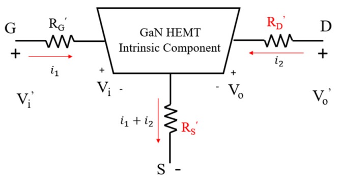
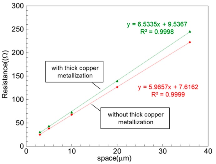
Copper-metallized gallium nitride (GaN) high-electron-mobility transistors (HEMTs) using a Ti/Pt/Ti diffusion barrier layer are fabricated and characterized for Ka-band applications. With a thick copper metallization layer of 6.8 μm adopted, the device exhibited a high output power density of 8.2 W/mm and a power-added efficiency (PAE) of 26% at 38 GHz. Such superior performance is mainly attributed to the substantial reduction of the source and drain resistance of the device. In addition to improvement in the Radio Frequency (RF) performance, the successful integration of the thick copper metallization in the device technology further reduces the manufacturing cost, making it extremely promising for future fifth-generation mobile communication system applications at millimeter-wave frequencies.

摘要

采用Ti/Pt/Ti扩散阻挡层的铜金属化氮化镓(GaN)高电子迁移率晶体管(HEMT)被制造出来并针对Ka波段应用进行了表征。采用6.8μm厚的铜金属化层时,该器件在38GHz频率下展现出8.2W/mm的高输出功率密度和26%的功率附加效率(PAE)。这种优异的性能主要归因于器件源极和漏极电阻的大幅降低。除了射频(RF)性能的提升外,厚铜金属化在器件技术中的成功集成进一步降低了制造成本,使其在毫米波频率的未来第五代移动通信系统应用中极具前景。

https://cdn.ncbi.nlm.nih.gov/pmc/blobs/833a/7074802/357211a5a225/micromachines-11-00222-g013.jpg
https://cdn.ncbi.nlm.nih.gov/pmc/blobs/833a/7074802/23796274d30b/micromachines-11-00222-g001.jpg
https://cdn.ncbi.nlm.nih.gov/pmc/blobs/833a/7074802/0378f706d034/micromachines-11-00222-g002.jpg
https://cdn.ncbi.nlm.nih.gov/pmc/blobs/833a/7074802/3d2d73f79e3d/micromachines-11-00222-g003.jpg
https://cdn.ncbi.nlm.nih.gov/pmc/blobs/833a/7074802/e5dcb22d2269/micromachines-11-00222-g004.jpg
https://cdn.ncbi.nlm.nih.gov/pmc/blobs/833a/7074802/210a65ec8177/micromachines-11-00222-g005.jpg
https://cdn.ncbi.nlm.nih.gov/pmc/blobs/833a/7074802/8428f21e5b61/micromachines-11-00222-g006.jpg
https://cdn.ncbi.nlm.nih.gov/pmc/blobs/833a/7074802/6238bd3e3c16/micromachines-11-00222-g007.jpg
https://cdn.ncbi.nlm.nih.gov/pmc/blobs/833a/7074802/fd10fef7e1f4/micromachines-11-00222-g008.jpg
https://cdn.ncbi.nlm.nih.gov/pmc/blobs/833a/7074802/f7b7a9307712/micromachines-11-00222-g009.jpg
https://cdn.ncbi.nlm.nih.gov/pmc/blobs/833a/7074802/ee75fad8f3e9/micromachines-11-00222-g010.jpg
https://cdn.ncbi.nlm.nih.gov/pmc/blobs/833a/7074802/5ee9a62d604c/micromachines-11-00222-g011.jpg
https://cdn.ncbi.nlm.nih.gov/pmc/blobs/833a/7074802/29e22bf2c4e7/micromachines-11-00222-g012.jpg
https://cdn.ncbi.nlm.nih.gov/pmc/blobs/833a/7074802/357211a5a225/micromachines-11-00222-g013.jpg

相似文献

1
Gallium Nitride (GaN) High-Electron-Mobility Transistors with Thick Copper Metallization Featuring a Power Density of 8.2 W/mm for Ka-Band Applications.用于Ka波段应用的具有厚铜金属化层、功率密度为8.2W/mm的氮化镓(GaN)高电子迁移率晶体管。
Micromachines (Basel). 2020 Feb 21;11(2):222. doi: 10.3390/mi11020222.
2
Improvement of AlGaN/GaN High-Electron-Mobility Transistor Radio Frequency Performance Using Ohmic Etching Patterns for Ka-Band Applications.用于Ka波段应用的欧姆蚀刻图案改善AlGaN/GaN高电子迁移率晶体管的射频性能
Micromachines (Basel). 2023 Dec 30;15(1):81. doi: 10.3390/mi15010081.
3
Adoption of the Wet Surface Treatment Technique for the Improvement of Device Performance of Enhancement-Mode AlGaN/GaN MOSHEMTs for Millimeter-Wave Applications.采用湿表面处理技术改善用于毫米波应用的增强型AlGaN/GaN MOSHEMT器件性能
Materials (Basel). 2021 Nov 1;14(21):6558. doi: 10.3390/ma14216558.
4
Thermal property evaluation of a 2.5D integration method with device level microchannel direct cooling for a high-power GaN HEMT device.用于高功率氮化镓高电子迁移率晶体管器件的具有器件级微通道直接冷却的2.5D集成方法的热性能评估
Microsyst Nanoeng. 2022 Nov 11;8:119. doi: 10.1038/s41378-022-00462-3. eCollection 2022.
5
Comparative analysis of nano-scale structural and electrical properties in AlGaN/GaN high electron mobility transistors on SiC and sapphire substrates.碳化硅和蓝宝石衬底上的AlGaN/GaN高电子迁移率晶体管的纳米级结构和电学特性的对比分析
J Nanosci Nanotechnol. 2013 Oct;13(10):7083-8. doi: 10.1166/jnn.2013.7631.
6
AlGaN/GaN on SiC Devices without a GaN Buffer Layer: Electrical and Noise Characteristics.碳化硅衬底上无氮化镓缓冲层的氮化铝镓/氮化镓器件:电学和噪声特性
Micromachines (Basel). 2020 Dec 20;11(12):1131. doi: 10.3390/mi11121131.
7
The Evolution of Manufacturing Technology for GaN Electronic Devices.氮化镓电子器件制造技术的发展
Micromachines (Basel). 2021 Jun 23;12(7):737. doi: 10.3390/mi12070737.
8
Improvement of AlGaN/GaN HEMTs Linearity Using Etched-Fin Gate Structure for Ka Band Applications.用于Ka波段应用的采用蚀刻鳍栅结构改善AlGaN/GaN高电子迁移率晶体管的线性度
Micromachines (Basel). 2023 Apr 25;14(5):931. doi: 10.3390/mi14050931.
9
An Overview of Normally-Off GaN-Based High Electron Mobility Transistors.基于氮化镓的常关型高电子迁移率晶体管概述。
Materials (Basel). 2019 May 15;12(10):1599. doi: 10.3390/ma12101599.
10
Effects of Thermal Boundary Resistance on Thermal Management of Gallium-Nitride-Based Semiconductor Devices: A Review.热边界电阻对氮化镓基半导体器件热管理的影响:综述
Micromachines (Basel). 2023 Nov 8;14(11):2076. doi: 10.3390/mi14112076.

引用本文的文献

1
Enhanced Conductivity of Multilayer Copper-Carbon Nanofilms via Plasma Immersion Deposition.通过等离子体浸没沉积提高多层铜-碳纳米薄膜的导电性
Nanomicro Lett. 2025 Feb 5;17(1):130. doi: 10.1007/s40820-024-01628-6.
2
Accessible chemical space for metal nitride perovskites.金属氮化物钙钛矿的可及化学空间。
Chem Sci. 2023 Aug 15;14(34):9175-9185. doi: 10.1039/d3sc02171h. eCollection 2023 Aug 30.
3
Influence of a Two-Dimensional Growth Mode on Electrical Properties of the GaN Buffer in an AlGaN/GaN High Electron Mobility Transistor.
二维生长模式对AlGaN/GaN高电子迁移率晶体管中GaN缓冲层电学性质的影响。
Materials (Basel). 2022 Sep 1;15(17):6043. doi: 10.3390/ma15176043.
4
A Novel GaN:C Millimeter-Wave HEMT with AlGaN Electron-Blocking Layer.一种具有AlGaN电子阻挡层的新型GaN:C毫米波高电子迁移率晶体管。
Materials (Basel). 2022 Jan 18;15(3):703. doi: 10.3390/ma15030703.
5
The Evolution of Manufacturing Technology for GaN Electronic Devices.氮化镓电子器件制造技术的发展
Micromachines (Basel). 2021 Jun 23;12(7):737. doi: 10.3390/mi12070737.
6
Editorial for the Special Issue on Wide Bandgap Based Devices: Design, Fabrication and Applications.基于宽带隙器件的特刊社论:设计、制造与应用
Micromachines (Basel). 2021 Jan 15;12(1):83. doi: 10.3390/mi12010083.
7
Large-Signal Linearity and High-Frequency Noise of Passivated AlGaN/GaN High-Electron Mobility Transistors.钝化AlGaN/GaN高电子迁移率晶体管的大信号线性度和高频噪声
Micromachines (Basel). 2020 Dec 24;12(1):7. doi: 10.3390/mi12010007.