Chen Xiong, Zhang Yu, Guan Xiangfeng, Zhang Hao
Organic optoelectronics research center in Fujian Universities, College of electronics and information science, Fujian Jiangxia University, Fuzhou 350108, China.
College of Materials Science and Engineering, Shanghai University, Shanghai 200444, China.
Nanomaterials (Basel). 2020 Apr 23;10(4):806. doi: 10.3390/nano10040806.
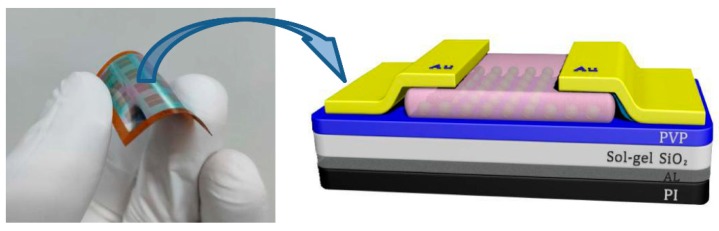
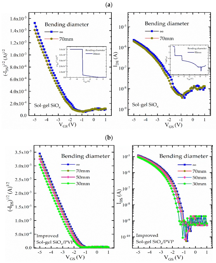
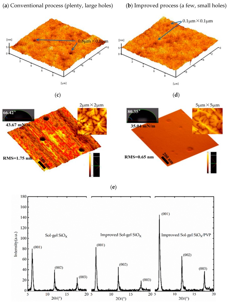
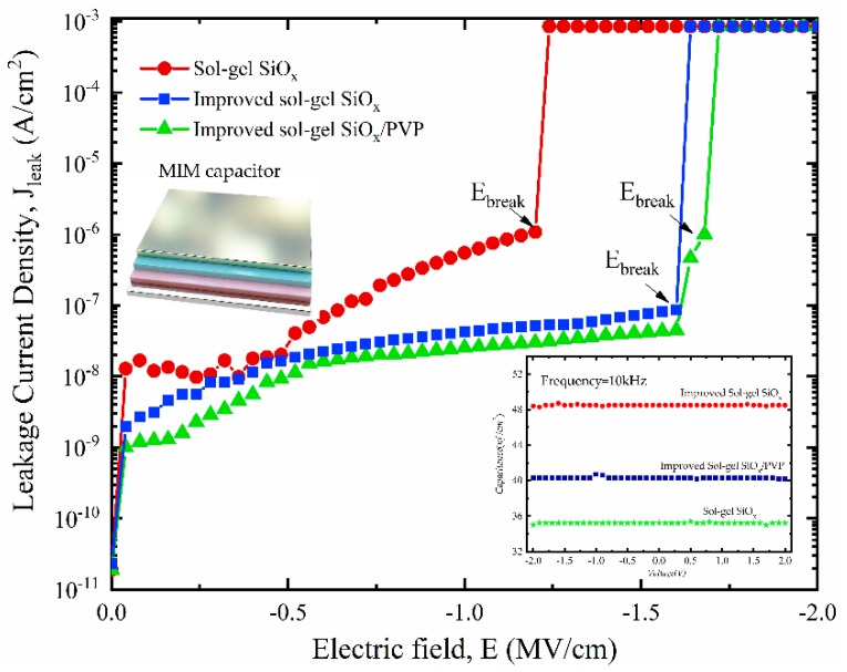
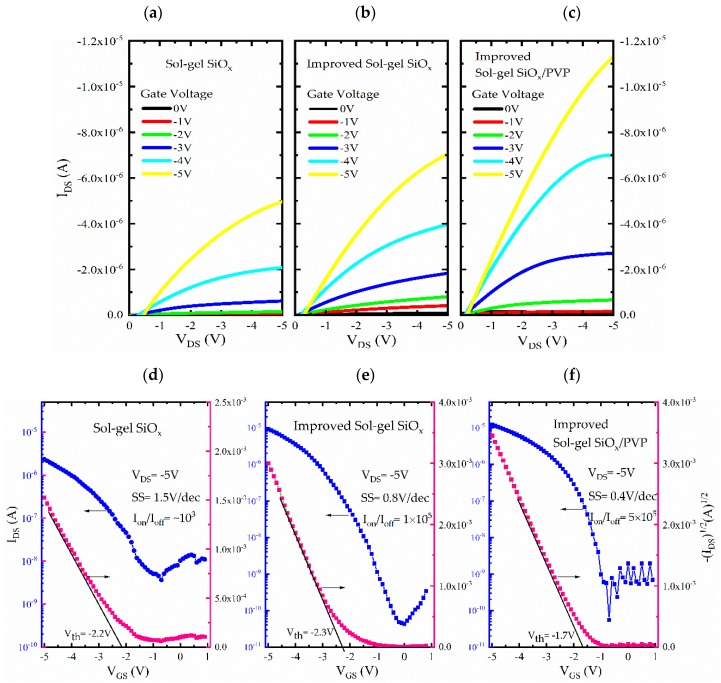
A high-quality dielectric layer is essential for organic thin-film transistors (OTFTs) operated at a low-power consumption level. In this study, a facile improved technique for the synthesis of solution-processed silica is proposed. By optimizing the synthesis and processing technique fewer pores were found on the surface of the film, particularly no large holes were observable after improving the annealing process, and the improved solution-gelation (sol-gel) SiO dielectric achieved a higher breakdown strength (1.6 MV/cm) and lower leakage current density (10 A/cm at 1.5 MV/cm). Consequently, a pentacene based OTFT with a high field effect mobility (1.8 cm/Vs), a low threshold voltage (-1.7 V), a steeper subthreshold slope (0.4 V/dec) and a relatively high on/off ratio (~10) was fabricated by applying a hybrid gate insulator which consisted of improved sol-gel SiO and polyvinyl phenol (PVP). This could be ascribed to both the high k of SiO and the smoother, hydrophobic dielectric surface with low trap density, which was proved by atomic force microscopy (AFM) and a water contact angle test, respectively. Additionally, we systematically studied and evaluated the stability of devices in the compressed state. The devices based on dielectric fabricated by conventional sol-gel processes were more susceptible to the curvature. While the improved device presented an excellent mechanic strength, it could still function at the higher bending compression without a significant degradation in performance. Thus, this solution-process technology provides an effective approach to fabricate high-quality dielectric and offers great potential for low-cost, fast and portable organic electronic applications.
对于在低功耗水平下工作的有机薄膜晶体管(OTFT)而言,高质量的介电层至关重要。在本研究中,提出了一种简便的改进技术用于合成溶液处理的二氧化硅。通过优化合成和处理技术,发现薄膜表面的孔隙较少,特别是在改进退火工艺后未观察到大洞,并且改进后的溶液凝胶法(sol - gel)SiO介电材料实现了更高的击穿强度(1.6 MV/cm)和更低的漏电流密度(在1.5 MV/cm时为10 A/cm)。因此,通过应用由改进的sol - gel SiO和聚乙烯基苯酚(PVP)组成的混合栅极绝缘体,制备了一种具有高场效应迁移率(约1.8 cm²/V·s)、低阈值电压(-1.7 V)、较陡的亚阈值斜率(约0.4 V/dec)和相对较高的开/关比(约10)的并五苯基OTFT。这可归因于SiO的高介电常数以及由原子力显微镜(AFM)和水接触角测试分别证明的具有低陷阱密度的更光滑、疏水的介电表面。此外,我们系统地研究和评估了器件在压缩状态下的稳定性。基于传统sol - gel工艺制备的介电材料的器件更容易受到曲率的影响。而改进后的器件表现出优异的机械强度,在更高的弯曲压缩下仍能正常工作且性能无明显下降。因此,这种溶液处理技术为制造高质量介电材料提供了一种有效方法,并为低成本、快速和便携式有机电子应用提供了巨大潜力。