Zhou Tianshen, Ma Shuying, Yu Daquan, Li Ming, Hang Tao
School of Materials Science and Engineering, Shanghai Jiao Tong University, Shanghai 200240, China.
Huatian Technology (Kunshan) Electronics Co., Ltd., Kunshan 215300, China.
Sensors (Basel). 2020 Jul 22;20(15):4077. doi: 10.3390/s20154077.
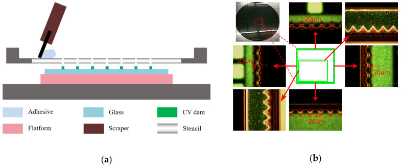
To meet the urgent market demand for small package size and high reliability performance for automotive CMOS image sensor (CIS) application, wafer level chip scale packaging (WLCSP) technology using through silicon vias (TSV) needs to be developed to replace current chip on board (COB) packages. In this paper, a WLCSP with the size of 5.82 mm × 5.22 mm and thickness of 850 μm was developed for the backside illumination (BSI) CIS chip using a 65 nm node with a size of 5.8 mm × 5.2 mm. The packaged product has 1392 × 976 pixels and a resolution of up to 60 frames per second with more than 120 dB dynamic range. The structure of the 3D package was designed and the key fabrication processes on a 12" inch wafer were investigated. More than 98% yield and excellent optical performance of the CIS package was achieved after process optimization. The final packages were qualified by AEC-Q100 Grade 2.
为满足汽车CMOS图像传感器(CIS)应用对小封装尺寸和高可靠性性能的迫切市场需求,需要开发采用硅通孔(TSV)的晶圆级芯片尺寸封装(WLCSP)技术来取代当前的板上芯片(COB)封装。本文针对尺寸为5.8 mm×5.2 mm的65 nm节点背照式(BSI)CIS芯片,开发了一种尺寸为5.82 mm×5.22 mm、厚度为850μm的WLCSP。封装后的产品具有1392×976像素,分辨率高达每秒60帧,动态范围超过120 dB。设计了3D封装结构,并研究了12英寸晶圆上的关键制造工艺。经过工艺优化,CIS封装的成品率超过98%,并具有优异的光学性能。最终封装产品通过了AEC-Q100 2级认证。