Dahiya Abhishek Singh, Shakthivel Dhayalan, Kumaresan Yogeenth, Zumeit Ayoub, Christou Adamos, Dahiya Ravinder
Bendable Electronics and Sensing Technologies (BEST) Group, University of Glasgow, Glasgow, G12 8QQ, UK.
Nano Converg. 2020 Oct 9;7(1):33. doi: 10.1186/s40580-020-00243-6.
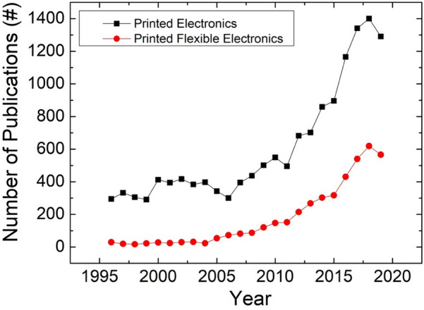
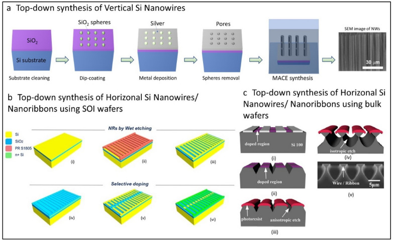
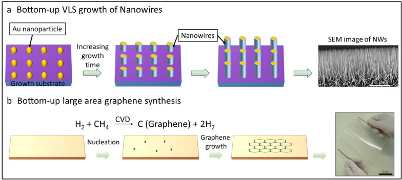
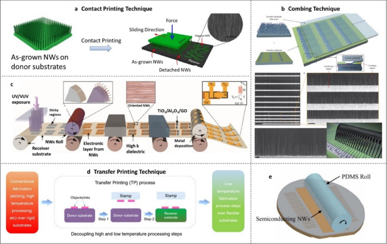
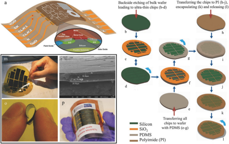
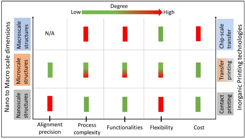
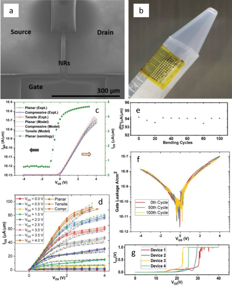
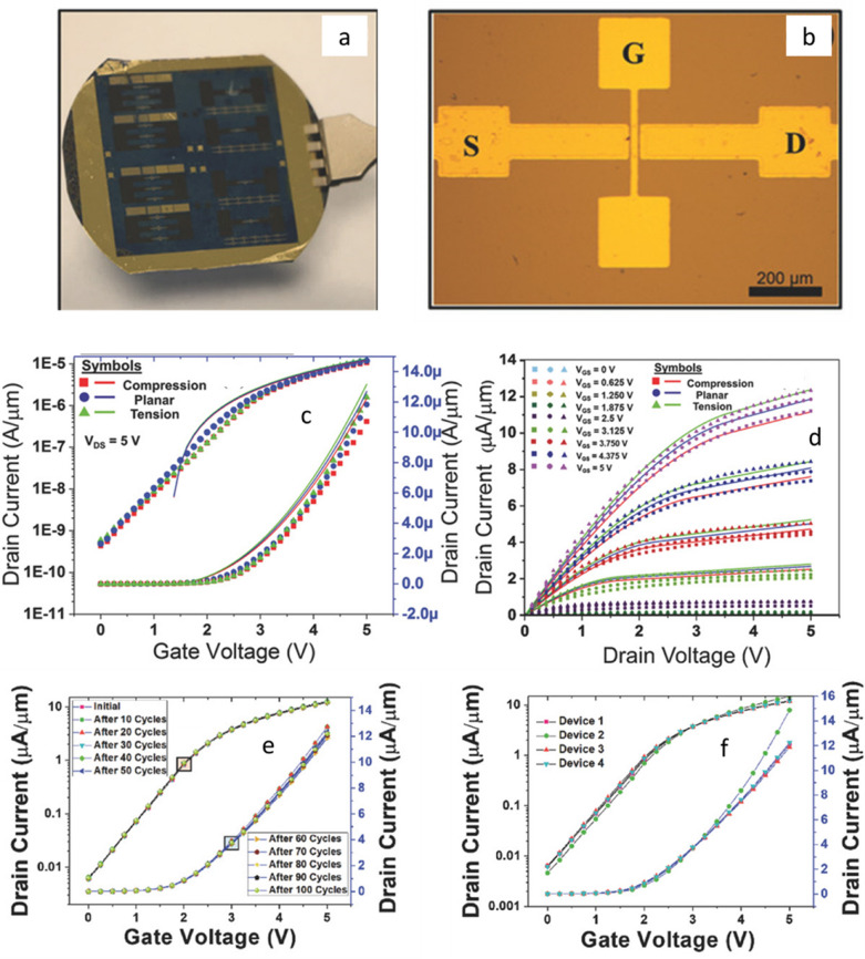
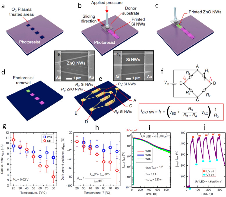
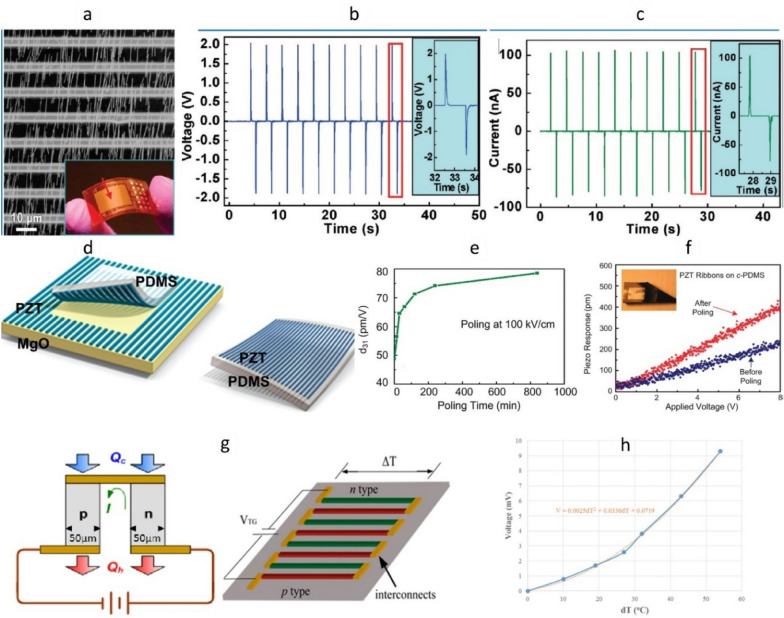
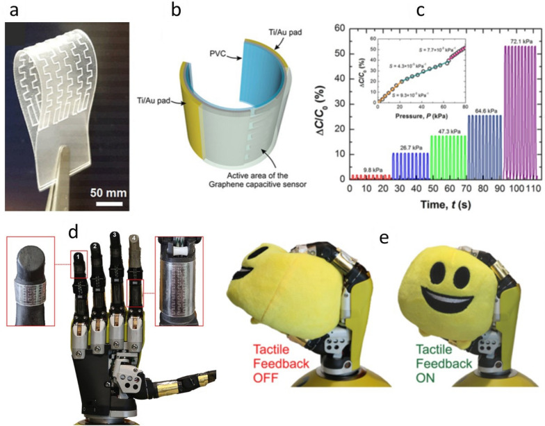
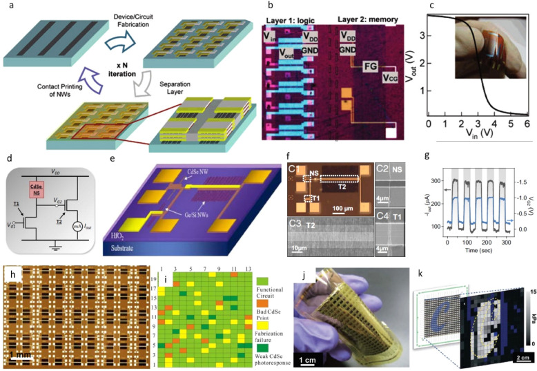
The Printed Electronics (PE) is expected to revolutionise the way electronics will be manufactured in the future. Building on the achievements of the traditional printing industry, and the recent advances in flexible electronics and digital technologies, PE may even substitute the conventional silicon-based electronics if the performance of printed devices and circuits can be at par with silicon-based devices. In this regard, the inorganic semiconducting materials-based approaches have opened new avenues as printed nano (e.g. nanowires (NWs), nanoribbons (NRs) etc.), micro (e.g. microwires (MWs)) and chip (e.g. ultra-thin chips (UTCs)) scale structures from these materials have been shown to have performances at par with silicon-based electronics. This paper reviews the developments related to inorganic semiconducting materials based high-performance large area PE, particularly using the two routes i.e. Contact Printing (CP) and Transfer Printing (TP). The detailed survey of these technologies for large area PE onto various unconventional substrates (e.g. plastic, paper etc.) is presented along with some examples of electronic devices and circuit developed with printed NWs, NRs and UTCs. Finally, we discuss the opportunities offered by PE, and the technical challenges and viable solutions for the integration of inorganic functional materials into large areas, 3D layouts for high throughput, and industrial-scale manufacturing using printing technologies.
印刷电子(PE)有望彻底改变未来电子产品的制造方式。基于传统印刷行业的成就以及柔性电子和数字技术的最新进展,如果印刷器件和电路的性能能够与硅基器件相媲美,PE甚至可能取代传统的硅基电子器件。在这方面,基于无机半导体材料的方法开辟了新途径,因为这些材料制成的印刷纳米(如纳米线(NWs)、纳米带(NRs)等)、微米(如微线(MWs))和芯片(如超薄芯片(UTCs))规模结构已被证明具有与硅基电子产品相当的性能。本文综述了基于无机半导体材料的高性能大面积印刷电子的发展情况,特别是采用接触印刷(CP)和转移印刷(TP)这两种途径。文中介绍了将这些大面积印刷电子技术应用于各种非传统基板(如塑料、纸张等)的详细情况,并列举了一些用印刷的纳米线、纳米带和超薄芯片开发的电子器件和电路的实例。最后,我们讨论了印刷电子带来的机遇,以及将无机功能材料集成到大面积、用于高通量的3D布局以及采用印刷技术进行工业规模制造所面临的技术挑战和可行解决方案。