• 文献检索
  • 文档翻译
  • 深度研究
  • 学术资讯
  • Suppr Zotero 插件Zotero 插件
  • 邀请有礼
  • 套餐&价格
  • 历史记录
应用&插件
Suppr Zotero 插件Zotero 插件浏览器插件Mac 客户端Windows 客户端微信小程序
定价
高级版会员购买积分包购买API积分包
服务
文献检索文档翻译深度研究API 文档MCP 服务
关于我们
关于 Suppr公司介绍联系我们用户协议隐私条款
关注我们

Suppr 超能文献

核心技术专利:CN118964589B侵权必究
粤ICP备2023148730 号-1Suppr @ 2026

文献检索

告别复杂PubMed语法,用中文像聊天一样搜索,搜遍4000万医学文献。AI智能推荐,让科研检索更轻松。

立即免费搜索

文件翻译

保留排版,准确专业,支持PDF/Word/PPT等文件格式,支持 12+语言互译。

免费翻译文档

深度研究

AI帮你快速写综述,25分钟生成高质量综述,智能提取关键信息,辅助科研写作。

立即免费体验

电感耦合等离子体溅射合成氮化钽薄膜的微观结构演变

Microstructural evolution of tantalum nitride thin films synthesized by inductively coupled plasma sputtering.

作者信息

Baik Sung-Il, Kim Young-Woon

机构信息

Research Institute of Advanced Materials, Department of Materials Science and Engineering, Seoul National University, 1 Gwanak-ro Gwanak-gu, Seoul, Republic of Korea.

Present address: Department of Materials Science & Engineering, Northwestern University, Evanston, IL, 60208, USA.

出版信息

Appl Microsc. 2020 Feb 27;50(1):7. doi: 10.1186/s42649-020-00026-7.

DOI:10.1186/s42649-020-00026-7
PMID:33580437
原文链接:https://pmc.ncbi.nlm.nih.gov/articles/PMC7818345/
Abstract

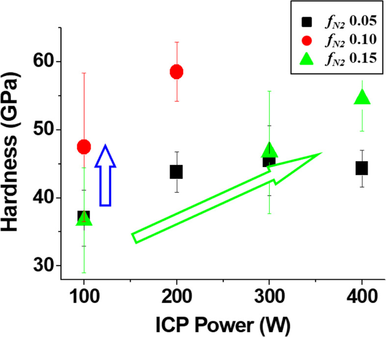
Tantalum nitride (TaN) thin films were grown utilizing an inductively coupled plasma (ICP) assisted direct current (DC) sputtering, and 20-100% improved microhardness values were obtained. The detailed microstructural changes of the TaN films were characterized utilizing transmission electron microscopy (TEM), as a function of nitrogen gas fraction and ICP power. As nitrogen gas fraction increases from 0.05 to 0.15, the TaN phase evolves from body-centered-cubic (b.c.c.) TaN, to face-centered-cubic (f.c.c.) δ-TaN, to hexagonal-close-packing (h.c.p.) ε-TaN phase. By increasing ICP power from 100 W to 400 W, the f.c.c. δ- TaN phase becomes the main phase in all nitrogen fractions investigated. The higher ICP power enhances the mobility of Ta and N ions, which stabilizes the δ-TaN phase like a high-temperature regime and removes the micro-voids between the columnar grains in the TaN film. The dense δ-TaN structure with reduced columnar grains and micro-voids increases the strength of the TaN film.

摘要

利用电感耦合等离子体(ICP)辅助直流(DC)溅射生长氮化钽(TaN)薄膜,并获得了提高20%-100%的显微硬度值。利用透射电子显微镜(TEM)对TaN薄膜的详细微观结构变化进行了表征,该变化是氮气分数和ICP功率的函数。随着氮气分数从0.05增加到0.15,TaN相从体心立方(b.c.c.)TaN演变为面心立方(f.c.c.)δ-TaN,再演变为六方密堆积(h.c.p.)ε-TaN相。通过将ICP功率从100W增加到400W,f.c.c.δ-TaN相在所有研究的氮分数中成为主相。较高的ICP功率提高了Ta和N离子的迁移率,这像在高温状态下一样稳定了δ-TaN相,并消除了TaN薄膜中柱状晶粒之间的微孔。具有减少的柱状晶粒和微孔的致密δ-TaN结构提高了TaN薄膜的强度。

https://cdn.ncbi.nlm.nih.gov/pmc/blobs/8e69/7818345/d71f4e0d3306/42649_2020_26_Fig7_HTML.jpg
https://cdn.ncbi.nlm.nih.gov/pmc/blobs/8e69/7818345/825e54d5d366/42649_2020_26_Fig1_HTML.jpg
https://cdn.ncbi.nlm.nih.gov/pmc/blobs/8e69/7818345/a9ea5a938766/42649_2020_26_Fig2_HTML.jpg
https://cdn.ncbi.nlm.nih.gov/pmc/blobs/8e69/7818345/9cabe2b44051/42649_2020_26_Fig3_HTML.jpg
https://cdn.ncbi.nlm.nih.gov/pmc/blobs/8e69/7818345/a653e680c065/42649_2020_26_Fig4_HTML.jpg
https://cdn.ncbi.nlm.nih.gov/pmc/blobs/8e69/7818345/5604def6dbfb/42649_2020_26_Fig5_HTML.jpg
https://cdn.ncbi.nlm.nih.gov/pmc/blobs/8e69/7818345/3936eb52868a/42649_2020_26_Fig6_HTML.jpg
https://cdn.ncbi.nlm.nih.gov/pmc/blobs/8e69/7818345/d71f4e0d3306/42649_2020_26_Fig7_HTML.jpg

相似文献

1
Microstructural evolution of tantalum nitride thin films synthesized by inductively coupled plasma sputtering.电感耦合等离子体溅射合成氮化钽薄膜的微观结构演变
Appl Microsc. 2020 Feb 27;50(1):7. doi: 10.1186/s42649-020-00026-7.
2
Low Resistivity Hafnium Nitride Thin Films Deposited by Inductively Coupled Plasma Assisted Magnetron Sputtering in Microelectronics.电感耦合等离子体辅助磁控溅射沉积的低电阻率氮化铪薄膜在微电子领域的应用
J Nanosci Nanotechnol. 2021 Jul 1;21(7):4129-4132. doi: 10.1166/jnn.2021.19216.
3
Effect of under-layer treatment of Ta/TaN barrier film on corrosion between Cu seed and Ta in chemical-mechanical-polishing slurry.Ta/TaN阻挡层薄膜的底层处理对化学机械抛光浆料中铜籽晶与Ta之间腐蚀的影响。
J Nanosci Nanotechnol. 2010 Jul;10(7):4196-203. doi: 10.1166/jnn.2010.2448.
4
Enhancement of the crystalline Ge film growth by inductively coupled plasma-assisted pulsed DC sputtering.通过电感耦合等离子体辅助脉冲直流溅射增强晶体锗薄膜的生长。
J Nanosci Nanotechnol. 2014 Nov;14(11):8567-71. doi: 10.1166/jnn.2014.9997.
5
Effect of Inductively Coupled Plasma on the Properties of Nanocrystalline Vanadium Nitride Films for Corrosion Resistant Surface.电感耦合等离子体对用于耐腐蚀表面的纳米晶氮化钒薄膜性能的影响。
J Nanosci Nanotechnol. 2018 Mar 1;18(3):2258-2261. doi: 10.1166/jnn.2018.14975.
6
Self-supported amorphous TaN(O)/nickel foam thin film as an advanced electrocatalyst for hydrogen evolution reaction.自支撑非晶态TaN(O)/泡沫镍薄膜作为析氢反应的先进电催化剂。
Chem Commun (Camb). 2022 Mar 8;58(20):3310-3313. doi: 10.1039/d2cc00151a.
7
Study of nitrogen diffusion profile of low resistivity diffusion barrier by resputtering technology.利用再溅射技术对低电阻率扩散阻挡层氮扩散分布的研究。
J Nanosci Nanotechnol. 2009 Feb;9(2):759-63. doi: 10.1166/jnn.2009.c019.
8
Preparation of taN thin film by H2 plasma assisted atomic layer deposition using tert-butylimino-tris-ethylmethylamino tantalum.使用叔丁基亚氨基三(乙基甲基氨基)钽通过氢等离子体辅助原子层沉积制备钽氮薄膜。
J Nanosci Nanotechnol. 2006 Nov;6(11):3392-5. doi: 10.1166/jnn.2006.018.
9
Superhard nanocrystalline titanium nitride films formed by inductively coupled plasma-assisted sputtering.通过电感耦合等离子体辅助溅射形成的超硬纳米晶氮化钛薄膜。
J Nanosci Nanotechnol. 2011 Aug;11(8):7378-81. doi: 10.1166/jnn.2011.4794.
10
The Structure and Properties of Inductively Coupled Plasma Assisted Magnetron Sputtered Nanocrystalline CrN Films for Bearings of Wind Power Systems.用于风力发电系统轴承的电感耦合等离子体辅助磁控溅射纳米晶CrN薄膜的结构与性能
J Nanosci Nanotechnol. 2015 Jan;15(1):532-5. doi: 10.1166/jnn.2015.8398.