• 文献检索
  • 文档翻译
  • 深度研究
  • 学术资讯
  • Suppr Zotero 插件Zotero 插件
  • 邀请有礼
  • 套餐&价格
  • 历史记录
应用&插件
Suppr Zotero 插件Zotero 插件浏览器插件Mac 客户端Windows 客户端微信小程序
定价
高级版会员购买积分包购买API积分包
服务
文献检索文档翻译深度研究API 文档MCP 服务
关于我们
关于 Suppr公司介绍联系我们用户协议隐私条款
关注我们

Suppr 超能文献

核心技术专利:CN118964589B侵权必究
粤ICP备2023148730 号-1Suppr @ 2026

文献检索

告别复杂PubMed语法,用中文像聊天一样搜索,搜遍4000万医学文献。AI智能推荐,让科研检索更轻松。

立即免费搜索

文件翻译

保留排版,准确专业,支持PDF/Word/PPT等文件格式,支持 12+语言互译。

免费翻译文档

深度研究

AI帮你快速写综述,25分钟生成高质量综述,智能提取关键信息,辅助科研写作。

立即免费体验

通过氯化钾电解质评估的用于制造均匀排列的液栅碳纳米管场效应晶体管的无化学物质且可扩展的工艺。

Chemical-free and scalable process for the fabrication of a uniform array of liquid-gated CNTFET, evaluated by KCl electrolyte.

作者信息

Agarwal Pankaj B, Thakur Navneet Kumar, Sharma Rishi, Singh Parul, Joseph Joshy, Tripura Chaturvedula

机构信息

Smart Sensors Area, CSIR-Central Electronics Engineering Research Institute (CSIR-CEERI), Pilani, Rajasthan, 333031, India.

Academy for Scientific and Innovative Research (AcSIR), Ghaziabad, Uttar Pradesh, 201002, India.

出版信息

Sci Rep. 2021 Feb 17;11(1):3979. doi: 10.1038/s41598-021-83451-2.

DOI:10.1038/s41598-021-83451-2
PMID:33597616
原文链接:https://pmc.ncbi.nlm.nih.gov/articles/PMC7889891/
Abstract

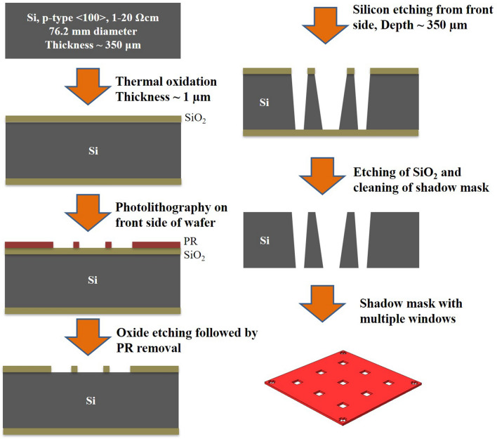
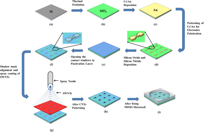
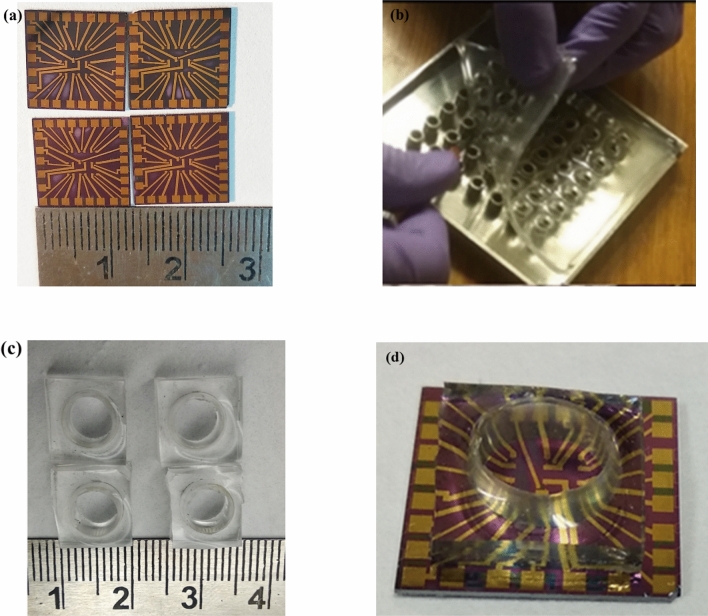
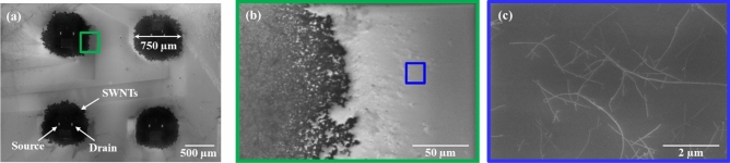
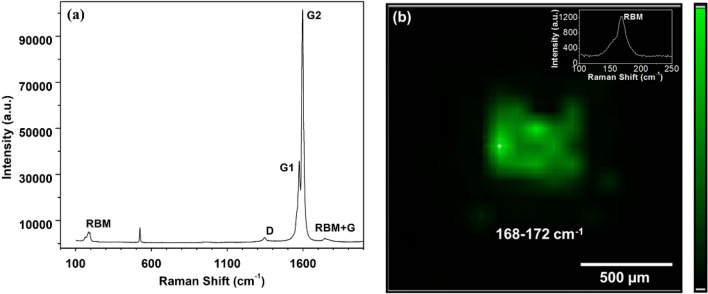
Biosensors based on liquid-gated carbon nanotubes field-effect transistors (LG-CNTFETs) have attracted considerable attention, as they offer high sensitivity and selectivity; quick response and label-free detection. However, their practical applications are limited due to the numerous fabrication challenges including resist-based lithography, in which after the lithography process, the resist leaves trace level contaminations over the CNTs that affect the performance of the fabricated biosensors. Here, we report the realization of LG-CNTFET devices using silicon shadow mask-based chemical-free lithography process on a 3-in. silicon wafer, yielding 21 sensor chips. Each sensor chip consists of 3 × 3 array of LG-CNTFET devices. Field emission scanning electron microscope (FESEM) and Raman mapping confirm the isolation of devices within the array chip having 9 individual devices. A reference electrode (Ag/AgCl) is used to demonstrate the uniformity of sensing performances among the fabricated LG-CNTFET devices in an array using different KCl molar solutions. The average threshold voltage (V) for all 9 devices varies from 0.46 to 0.19 V for 0.1 mM to 1 M KCl concentration range. This developed chemical-free process of LG-CNTFET array fabrication is simple, inexpensive, rapid having a commercial scope and thus opens a new realm of scalable realization of various biosensors.

摘要

基于液栅碳纳米管场效应晶体管(LG-CNTFET)的生物传感器因其具有高灵敏度和选择性、快速响应以及无需标记检测等优点而备受关注。然而,由于存在诸多制造挑战,包括基于光刻胶的光刻技术,在光刻过程之后,光刻胶会在碳纳米管上留下痕量污染物,从而影响所制造生物传感器的性能,其实际应用受到限制。在此,我们报告了在3英寸硅片上使用基于硅阴影掩膜的无化学光刻工艺实现LG-CNTFET器件,共得到21个传感器芯片。每个传感器芯片由3×3阵列的LG-CNTFET器件组成。场发射扫描电子显微镜(FESEM)和拉曼映射证实了阵列芯片内具有9个独立器件的器件隔离情况。使用参比电极(Ag/AgCl)来证明在使用不同KCl摩尔溶液的阵列中所制造的LG-CNTFET器件之间传感性能的均匀性。对于0.1 mM至1 M KCl浓度范围,所有9个器件的平均阈值电压(V)从0.46 V变化到0.19 V。这种所开发的LG-CNTFET阵列制造的无化学工艺简单、廉价、快速且具有商业应用前景,从而为各种生物传感器的可扩展实现开辟了一个新领域。

https://cdn.ncbi.nlm.nih.gov/pmc/blobs/cd92/7889891/d925786ab6b3/41598_2021_83451_Fig9_HTML.jpg
https://cdn.ncbi.nlm.nih.gov/pmc/blobs/cd92/7889891/7d75a84b71c3/41598_2021_83451_Fig1_HTML.jpg
https://cdn.ncbi.nlm.nih.gov/pmc/blobs/cd92/7889891/b7026fceaf20/41598_2021_83451_Fig2_HTML.jpg
https://cdn.ncbi.nlm.nih.gov/pmc/blobs/cd92/7889891/905404f1e14a/41598_2021_83451_Fig3_HTML.jpg
https://cdn.ncbi.nlm.nih.gov/pmc/blobs/cd92/7889891/bb9c66eb510c/41598_2021_83451_Fig4_HTML.jpg
https://cdn.ncbi.nlm.nih.gov/pmc/blobs/cd92/7889891/1ddcbfa92668/41598_2021_83451_Fig5_HTML.jpg
https://cdn.ncbi.nlm.nih.gov/pmc/blobs/cd92/7889891/7dfa59ba2dd5/41598_2021_83451_Fig6_HTML.jpg
https://cdn.ncbi.nlm.nih.gov/pmc/blobs/cd92/7889891/06234e8ea1db/41598_2021_83451_Fig7_HTML.jpg
https://cdn.ncbi.nlm.nih.gov/pmc/blobs/cd92/7889891/e506d3bf3f38/41598_2021_83451_Fig8_HTML.jpg
https://cdn.ncbi.nlm.nih.gov/pmc/blobs/cd92/7889891/d925786ab6b3/41598_2021_83451_Fig9_HTML.jpg

相似文献

1
Chemical-free and scalable process for the fabrication of a uniform array of liquid-gated CNTFET, evaluated by KCl electrolyte.通过氯化钾电解质评估的用于制造均匀排列的液栅碳纳米管场效应晶体管的无化学物质且可扩展的工艺。
Sci Rep. 2021 Feb 17;11(1):3979. doi: 10.1038/s41598-021-83451-2.
2
Dielectrophoresis-Based Positioning of Carbon Nanotubes for Wafer-Scale Fabrication of Carbon Nanotube Devices.基于介电泳的碳纳米管定位用于碳纳米管器件的晶圆级制造。
Micromachines (Basel). 2020 Dec 25;12(1):12. doi: 10.3390/mi12010012.
3
Intense pH Sensitivity Modulation in Carbon Nanotube-Based Field-Effect Transistor by Non-Covalent Polyfluorene Functionalization.通过非共价聚芴功能化实现基于碳纳米管的场效应晶体管中强烈的pH敏感性调制。
Nanomaterials (Basel). 2023 Mar 24;13(7):1157. doi: 10.3390/nano13071157.
4
Dielectrophoresis-Assisted Integration of 1024 Carbon Nanotube Sensors into a CMOS Microsystem.介电泳辅助集成 1024 个碳纳米管传感器到 CMOS 微系统中。
Adv Mater. 2017 May;29(17). doi: 10.1002/adma.201606852. Epub 2017 Mar 15.
5
High-performance printed carbon nanotube thin-film transistors array fabricated by a nonlithography technique using hafnium oxide passivation layer and mask.采用氧化铪钝化层和掩模的非光刻技术制造高性能印刷碳纳米管薄膜晶体管阵列。
ACS Appl Mater Interfaces. 2012 Dec;4(12):7047-54. doi: 10.1021/am302431e. Epub 2012 Dec 7.
6
Silicon Shadow Mask Technology for Aligning and Sorting of Semiconducting SWNTs for Sensitivity Enhancement: A Case Study of NO Gas Sensor.用于对准和分选半导体单壁碳纳米管以提高灵敏度的硅阴影掩膜技术:以NO气体传感器为例
ACS Appl Mater Interfaces. 2020 Sep 9;12(36):40901-40909. doi: 10.1021/acsami.0c10189. Epub 2020 Aug 26.
7
Scalable Production of High-Sensitivity, Label-Free DNA Biosensors Based on Back-Gated Graphene Field Effect Transistors.基于背栅式石墨烯场效应晶体管的高灵敏度、无标记 DNA 生物传感器的可扩展制造。
ACS Nano. 2016 Sep 27;10(9):8700-4. doi: 10.1021/acsnano.6b04110. Epub 2016 Sep 2.
8
Additive Influence of Top Metal Contact and Alumina Deposition on the Threshold Voltage of Suspended Carbon Nanotube Field-Effect Transistors.顶部金属接触和氧化铝沉积对悬浮碳纳米管场效应晶体管阈值电压的叠加影响
ACS Omega. 2023 Jul 19;8(30):27697-27702. doi: 10.1021/acsomega.3c03602. eCollection 2023 Aug 1.
9
Electrolyte-Gated Carbon Nanotube Field-Effect Transistor-Based Sensors for Nanoplastics Detection in Seawater: A Study of the Interaction between Nanoplastics and Carbon Nanotubes.基于电解质门控碳纳米管场效应晶体管的海水纳米塑料检测传感器:纳米塑料与碳纳米管相互作用的研究
ACS Appl Mater Interfaces. 2024 Jul 24;16(29):38768-38779. doi: 10.1021/acsami.4c07692. Epub 2024 Jul 12.
10
Wafer-Scale Uniform Carbon Nanotube Transistors for Ultrasensitive and Label-Free Detection of Disease Biomarkers.用于超灵敏且无标记检测疾病生物标志物的晶圆级均匀碳纳米管晶体管
ACS Nano. 2020 Jul 28;14(7):8866-8874. doi: 10.1021/acsnano.0c03523. Epub 2020 Jun 25.

引用本文的文献

1
Fabrication and Functionalisation of Nanocarbon-Based Field-Effect Transistor Biosensors.基于纳米碳的场效应晶体管生物传感器的制作与功能化。
Chembiochem. 2022 Dec 5;23(23):e202200282. doi: 10.1002/cbic.202200282. Epub 2022 Nov 3.

本文引用的文献

1
Silicon Shadow Mask Technology for Aligning and Sorting of Semiconducting SWNTs for Sensitivity Enhancement: A Case Study of NO Gas Sensor.用于对准和分选半导体单壁碳纳米管以提高灵敏度的硅阴影掩膜技术:以NO气体传感器为例
ACS Appl Mater Interfaces. 2020 Sep 9;12(36):40901-40909. doi: 10.1021/acsami.0c10189. Epub 2020 Aug 26.
2
Back-gated spray-deposited carbon nanotube thin film transistors operated in electrolytic solutions: an assessment towards future biosensing applications.在电解液中运行的背栅喷雾沉积碳纳米管薄膜晶体管:对未来生物传感应用的评估
J Mater Chem B. 2013 Aug 21;1(31):3797-3802. doi: 10.1039/c3tb20170h. Epub 2013 May 13.
3
Monolithic CMOS sensor platform featuring an array of 9'216 carbon-nanotube-sensor elements and low-noise, wide-bandwidth and wide-dynamic-range readout circuitry.
具有9216个碳纳米管传感器元件阵列以及低噪声、宽带宽和宽动态范围读出电路的单片CMOS传感器平台。
Sens Actuators B Chem. 2019 Jan 15;279:255-266. doi: 10.1016/j.snb.2018.10.004.
4
Electrically Controllable Single-Point Covalent Functionalization of Spin-Cast Carbon-Nanotube Field-Effect Transistor Arrays.电可控的旋涂碳纳米管场效应晶体管阵列单点共价功能化。
ACS Nano. 2018 Oct 23;12(10):9922-9930. doi: 10.1021/acsnano.8b03073. Epub 2018 Oct 3.
5
Ambient Processed, Water-Stable, Aqueous-Gated sub 1 V n-type Carbon Nanotube Field Effect Transistor.环境处理、水稳定、水门控的亚1伏n型碳纳米管场效应晶体管
Sci Rep. 2018 Jul 30;8(1):11386. doi: 10.1038/s41598-018-29882-w.
6
Inkjet Printing of High Performance Transistors with Micron Order Chemically Set Gaps.具有微米级化学设定间隙的高性能晶体管的喷墨打印。
Sci Rep. 2017 Apr 26;7(1):1202. doi: 10.1038/s41598-017-01391-2.
7
Inkjet Printing of Carbon Nanotubes.碳纳米管的喷墨打印
Nanomaterials (Basel). 2013 Jul 29;3(3):453-468. doi: 10.3390/nano3030453.
8
Selective ion-sensing with membrane-functionalized electrolyte-gated carbon nanotube field-effect transistors.采用膜功能化电解质门控碳纳米管场效应晶体管进行选择性离子传感。
Analyst. 2014 Oct 7;139(19):4947-54. doi: 10.1039/c4an00714j.
9
Arrays of single-walled carbon nanotubes with full surface coverage for high-performance electronics.具有全覆盖表面的单壁碳纳米管阵列,可实现高性能电子学。
Nat Nanotechnol. 2013 Mar;8(3):180-6. doi: 10.1038/nnano.2012.257. Epub 2013 Jan 27.
10
High-performance printed carbon nanotube thin-film transistors array fabricated by a nonlithography technique using hafnium oxide passivation layer and mask.采用氧化铪钝化层和掩模的非光刻技术制造高性能印刷碳纳米管薄膜晶体管阵列。
ACS Appl Mater Interfaces. 2012 Dec;4(12):7047-54. doi: 10.1021/am302431e. Epub 2012 Dec 7.