Gole Matthew T, Yin Zhewen, Wang Michael Cai, Lin Wayne, Zhou Ziran, Leem Juyoung, Takekuma Satoshi, Murphy Catherine J, Nam SungWoo
Department of Chemistry, University of Illinois at Urbana-Champaign, Urbana, IL, USA.
Department of Mechanical Engineering, University of South Florida, Tampa, FL, USA.
Sci Rep. 2021 Jun 10;11(1):12232. doi: 10.1038/s41598-021-91697-z.
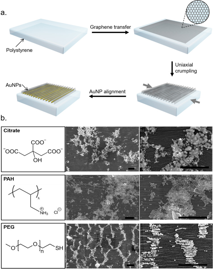
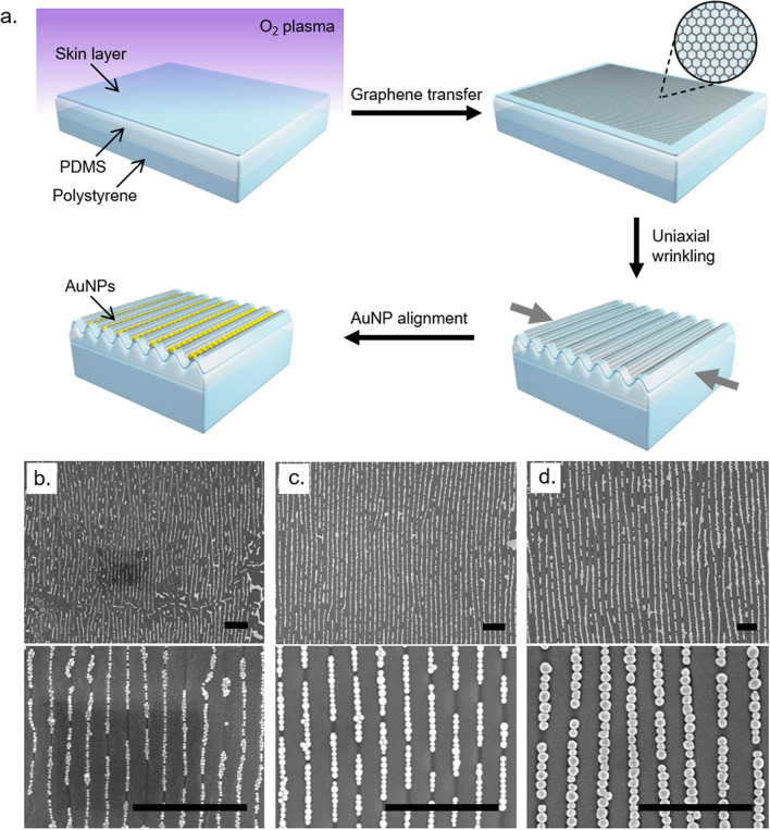
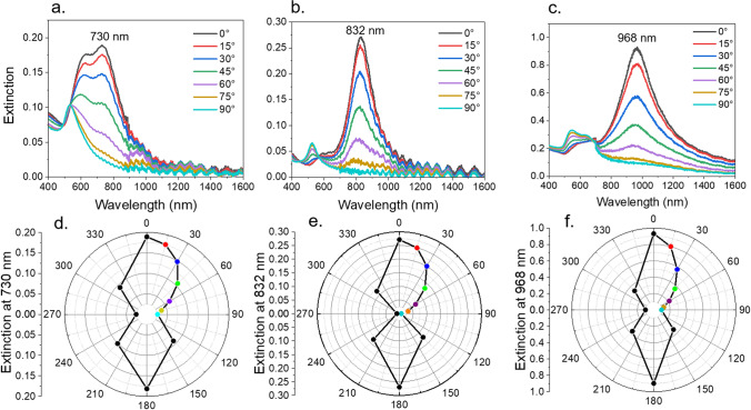
Hierarchical heterostructures of two-dimensional (2D) nanomaterials are versatile platforms for nanoscale optoelectronics. Further coupling of these 2D materials with plasmonic nanostructures, especially in non-close-packed morphologies, imparts new metastructural properties such as increased photosensitivity as well as spectral selectivity and range. However, the integration of plasmonic nanoparticles with 2D materials has largely been limited to lithographic patterning and/or undefined deposition of metallic structures. Here we show that colloidally synthesized zero-dimensional (0D) gold nanoparticles of various sizes can be deterministically self-assembled in highly-ordered, anisotropic, non-close-packed, multi-scale morphologies with templates designed from instability-driven, deformed 2D nanomaterials. The anisotropic plasmonic coupling of the particle arrays exhibits emergent polarization-dependent absorbance in the visible to near-IR regions. Additionally, controllable metasurface arrays of nanoparticles by functionalization with varying polymer brushes modulate the plasmonic coupling between polarization dependent and independent assemblies. This self-assembly method shows potential for bottom-up nanomanufacturing of diverse optoelectronic components and can potentially be adapted to a wide array of nanoscale 0D, 1D, and 2D materials.
二维(2D)纳米材料的分层异质结构是纳米级光电子学的多功能平台。这些二维材料与等离子体纳米结构的进一步耦合,特别是在非紧密堆积形态中,赋予了新的亚结构特性,如提高的光敏性以及光谱选择性和范围。然而,等离子体纳米颗粒与二维材料的集成在很大程度上仅限于光刻图案化和/或金属结构的不确定沉积。在这里,我们展示了各种尺寸的胶体合成零维(0D)金纳米颗粒可以通过由不稳定性驱动的变形二维纳米材料设计的模板,以高度有序、各向异性、非紧密堆积、多尺度形态确定性地自组装。粒子阵列的各向异性等离子体耦合在可见光到近红外区域表现出新兴的偏振相关吸光度。此外,通过用不同的聚合物刷进行功能化来控制纳米颗粒的超表面阵列,可调节偏振相关和独立组件之间的等离子体耦合。这种自组装方法显示了自下而上纳米制造各种光电子组件的潜力,并且有可能适用于各种纳米级0D、1D和2D材料。