School of Mechanical Engineering, Pusan National University, 63-2 Busan University-Ro, Geumjeong-gu, Busan, 46241, South Korea.
Department of Mechanical Engineering (Integrated Engineering Program), Kyung Hee University, 1732 Deogyeong-daero, Yongin, Gyeonggi, 17104, South Korea.
Sci Rep. 2021 Nov 2;11(1):21437. doi: 10.1038/s41598-021-01043-6.
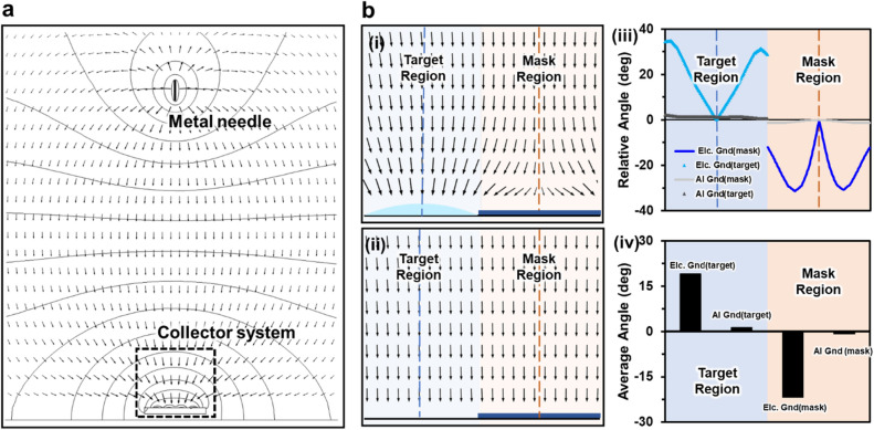
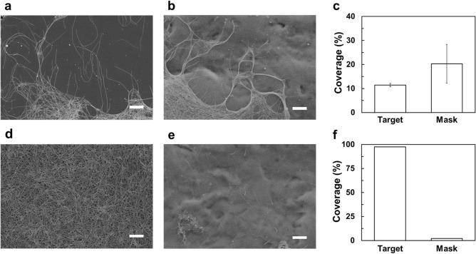
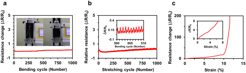
A patterned transparent electrode is a crucial component of state-of-the-art wearable devices and optoelectronic devices. However, most of the patterning methods using silver nanowires (AgNWs), which is one of the outstanding candidate materials for the transparent electrode, wasted a large amount of unused AgNWs during the patterning process. Here, we report a highly efficient patterning of AgNWs using electrospray deposition with grounded electrolyte solution (EDGE). During electrospray deposition, a patterned electrolyte solution collector attracted AgNWs by strong electrostatic attraction and selectively deposited them only on the patterned collector, minimizing AgNW deposited elsewhere. The enhanced patterning efficiency was verified through a comparison between the EDGE and conventional process by numerical simulation and experimental validation. As a result, despite the same electrospray deposition conditions for both cases except for the existence of the electrolyte solution collector, the coverage ratio of AgNWs fabricated by the EDGE process was at least six times higher than that of AgNWs produced by the conventional process. Furthermore, the EDGE process provided high design flexibility in terms of not only the material of the substrate, including a polymer and a ceramic but also the shape of the substrate, including a 2D flat and 3D curved surface. As an application of the EDGE process, a self-powered touch sensor exploiting the triboelectric effect was demonstrated. Thus, the EDGE process would be utilized in further application in wearable or implantable devices in the field of biomedicine, intelligent robots, and human-machine interface.
图案化透明电极是最先进的可穿戴设备和光电设备的关键组成部分。然而,大多数使用银纳米线(AgNWs)的图案化方法,AgNWs 是透明电极的杰出候选材料之一,在图案化过程中浪费了大量未使用的 AgNWs。在这里,我们报告了一种使用带接地电解质溶液的静电喷涂沉积(EDGE)进行高效 AgNWs 图案化的方法。在静电喷涂沉积过程中,图案化的电解质溶液收集器通过强静电吸引力吸引 AgNWs,并选择性地仅将其沉积在图案化的收集器上,最大限度地减少了沉积在其他地方的 AgNWs。通过数值模拟和实验验证,比较了 EDGE 和传统工艺的结果,验证了增强的图案化效率。结果表明,尽管两种情况下的静电喷涂沉积条件相同,除了电解质溶液收集器的存在外,EDGE 工艺制备的 AgNWs 的覆盖率至少是传统工艺的六倍。此外,EDGE 工艺在基板材料方面提供了高度的设计灵活性,不仅包括聚合物和陶瓷,还包括基板的形状,包括 2D 平面和 3D 曲面。作为 EDGE 工艺的应用,展示了一种利用摩擦电效应的自供电触摸传感器。因此,EDGE 工艺将在生物医学、智能机器人和人机界面等领域的可穿戴或植入式设备的进一步应用中得到利用。