• 文献检索
  • 文档翻译
  • 深度研究
  • 学术资讯
  • Suppr Zotero 插件Zotero 插件
  • 邀请有礼
  • 套餐&价格
  • 历史记录
应用&插件
Suppr Zotero 插件Zotero 插件浏览器插件Mac 客户端Windows 客户端微信小程序
定价
高级版会员购买积分包购买API积分包
服务
文献检索文档翻译深度研究API 文档MCP 服务
关于我们
关于 Suppr公司介绍联系我们用户协议隐私条款
关注我们

Suppr 超能文献

核心技术专利:CN118964589B侵权必究
粤ICP备2023148730 号-1Suppr @ 2026

文献检索

告别复杂PubMed语法,用中文像聊天一样搜索,搜遍4000万医学文献。AI智能推荐,让科研检索更轻松。

立即免费搜索

文件翻译

保留排版,准确专业,支持PDF/Word/PPT等文件格式,支持 12+语言互译。

免费翻译文档

深度研究

AI帮你快速写综述,25分钟生成高质量综述,智能提取关键信息,辅助科研写作。

立即免费体验

半导体WS的化学剥离效果及其在增材制造的异质结构石墨烯-WS-石墨烯光电二极管中的应用。

Chemical exfoliation efficacy of semiconducting WS and its use in an additively manufactured heterostructure graphene-WS-graphene photodiode.

作者信息

Desai Jay A, Adhikari Nirmal, Kaul Anupama B

机构信息

Department of Metallurgical, Materials and Biomedical Engineering, University of Texas at El Paso El Paso TX 79968 USA

Department of Material Science and Engineering Denton TX 76203 USA.

出版信息

RSC Adv. 2019 Aug 16;9(44):25805-25816. doi: 10.1039/c9ra03644j. eCollection 2019 Aug 13.

DOI:10.1039/c9ra03644j
PMID:35530073
原文链接:https://pmc.ncbi.nlm.nih.gov/articles/PMC9070084/
Abstract

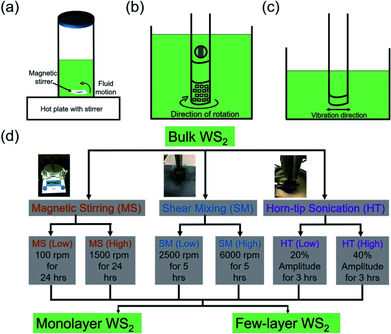
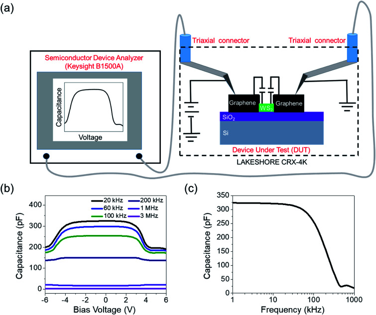
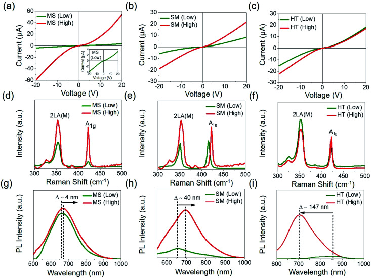
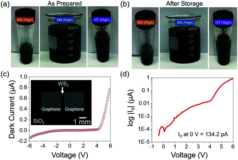
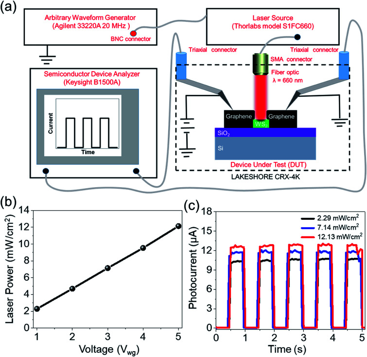
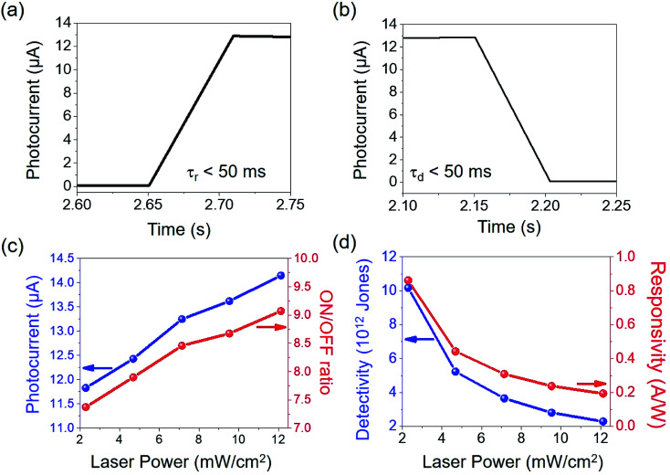
In the present work, various chemical exfoliation routes for semiconducting two-dimensional (2D) layered material WS are explored, which include magnetic stirring (MS), shear mixing (SM), and horn-tip (HT) sonication. Current-voltage measurements, Raman spectroscopy, and photoluminescence (PL) spectroscopy were used to characterize the drop-casted WS nanosheets produced by these three techniques and our analysis revealed that HT sonication produced the most optimal dispersions. Heterostructure photodetector devices were then fabricated using inkjet printing of the HT sonicated dispersions of WS and graphene. The photodetector device performance was measured using a stream of ON/OFF light pulses generated using a red laser with wavelength ∼ 660 nm, and an arbitrary waveform generator. From this analysis, the photoresponsivity and detectivity of the graphene-WS-graphene heterostructure devices were calculated to be ∼0.86 A W and ∼10 Jones, respectively. Capacitance-voltage (-) and -frequency () measurements were also conducted, where the was swept from -6 V to +6 V, while the change in was measured from ∼ 20 kHz up to 3 MHz to gain insights into the nature of the graphene-WS interface. From the - measurements, the plateaued at ∼324.3 pF from ∼-4 V to +4 V for the lowest of 20 kHz and it reduced to ∼200 pF from -6 V to ∼-4 V, and similarly from ∼4 V to 6 V, was ∼190 pF. The decrease in for > +4 V and < -4 V was attributed to the reduction of the interfacial barrier at the electrodes which is suggestive of a Schottky-based photodiode at the graphene-WS interface. A sharp decrease in from ∼315.75 pF at 25.76 kHz to ∼23.79 pF at 480 kHz (at 0 V bias) from the - measurements suggests a strong effect of interface trap density on built-up at the graphene-WS interface and the ensuing Schottky barrier height. Our work confirms the excellent potential of solution-cast, trilayer graphene-WS-graphene heterostructures as a promising photodetector platform using additively manufactured inkjet printing.

摘要

在本工作中,探索了用于半导体二维(2D)层状材料WS的各种化学剥离途径,其中包括磁力搅拌(MS)、剪切混合(SM)和喇叭尖(HT)超声处理。使用电流-电压测量、拉曼光谱和光致发光(PL)光谱对通过这三种技术制备的滴铸WS纳米片进行表征,我们的分析表明,HT超声处理产生了最理想的分散体。然后使用喷墨打印HT超声处理的WS和石墨烯分散体制备异质结构光电探测器器件。使用由波长约660 nm的红色激光和任意波形发生器产生的开/关光脉冲流测量光电探测器器件的性能。通过该分析,计算出石墨烯-WS-石墨烯异质结构器件的光响应度和探测率分别约为0.86 A/W和约10琼斯。还进行了电容-电压(-)和-频率()测量,其中将从-6 V扫描到+6 V,同时测量从约20 kHz到3 MHz的变化,以深入了解石墨烯-WS界面的性质。从-测量结果来看,在最低频率20 kHz时,从约-4 V到+4 V,约为324.3 pF并趋于平稳,从-6 V到约-4 V以及类似地从约4 V到6 V,约为190 pF。对于> +4 V和< -4 V时的降低归因于电极处界面势垒的降低,这表明在石墨烯-WS界面处存在基于肖特基的光电二极管。从-测量结果来看,在0 V偏压下,从25.76 kHz时的约315.75 pF急剧下降到480 kHz时的约23.79 pF,这表明界面陷阱密度对在石墨烯-WS界面处积累的以及随之而来的肖特基势垒高度有很强的影响。我们的工作证实了溶液浇铸的三层石墨烯-WS-石墨烯异质结构作为使用增材制造喷墨打印的有前景的光电探测器平台的巨大潜力。

https://cdn.ncbi.nlm.nih.gov/pmc/blobs/3d99/9070084/5ba1f0543525/c9ra03644j-f6.jpg
https://cdn.ncbi.nlm.nih.gov/pmc/blobs/3d99/9070084/89ca1ff8d0f6/c9ra03644j-f1.jpg
https://cdn.ncbi.nlm.nih.gov/pmc/blobs/3d99/9070084/0913f65e2ed2/c9ra03644j-f2.jpg
https://cdn.ncbi.nlm.nih.gov/pmc/blobs/3d99/9070084/b6595a3e7e64/c9ra03644j-f3.jpg
https://cdn.ncbi.nlm.nih.gov/pmc/blobs/3d99/9070084/1627ae75fc1a/c9ra03644j-f4.jpg
https://cdn.ncbi.nlm.nih.gov/pmc/blobs/3d99/9070084/037c0f8c0f70/c9ra03644j-f5.jpg
https://cdn.ncbi.nlm.nih.gov/pmc/blobs/3d99/9070084/5ba1f0543525/c9ra03644j-f6.jpg

相似文献

1
Chemical exfoliation efficacy of semiconducting WS and its use in an additively manufactured heterostructure graphene-WS-graphene photodiode.半导体WS的化学剥离效果及其在增材制造的异质结构石墨烯-WS-石墨烯光电二极管中的应用。
RSC Adv. 2019 Aug 16;9(44):25805-25816. doi: 10.1039/c9ra03644j. eCollection 2019 Aug 13.
2
Two-Dimensional CsAgBiBr/WS Heterostructure-Based Photodetector with Boosted Detectivity via Interfacial Engineering.基于二维CsAgBiBr/WS异质结构的光电探测器:通过界面工程提高探测率
ACS Nano. 2022 Mar 22;16(3):3985-3993. doi: 10.1021/acsnano.1c09513. Epub 2022 Feb 18.
3
Plasmonic WS Nanodiscs/Graphene van der Waals Heterostructure Photodetectors.等离子体 WS 纳米盘/石墨烯范德华异质结构光电探测器。
ACS Appl Mater Interfaces. 2019 Sep 11;11(36):33390-33398. doi: 10.1021/acsami.9b09262. Epub 2019 Sep 3.
4
High-Responsivity Gate-Tunable Ultraviolet-Visible Broadband Phototransistor Based on Graphene-WS Mixed-Dimensional (2D-0D) Heterostructure.基于石墨烯-WS混合维度(二维-零维)异质结构的高响应度栅极可调紫外-可见宽带光电晶体管。
ACS Appl Mater Interfaces. 2022 Feb 2;14(4):5775-5784. doi: 10.1021/acsami.1c18999. Epub 2022 Jan 23.
5
Improved liquid phase exfoliation technique for the fabrication of MoS/graphene heterostructure-based photodetector.用于制备基于MoS/石墨烯异质结构光电探测器的改进液相剥离技术
Heliyon. 2024 Jan 26;10(3):e24964. doi: 10.1016/j.heliyon.2024.e24964. eCollection 2024 Feb 15.
6
A high performance self-powered photodetector based on a 1D Te-2D WS mixed-dimensional heterostructure.一种基于一维碲-二维硫化钨混合维度异质结构的高性能自供电光电探测器。
Nanoscale Adv. 2021 Mar 15;3(9):2657-2665. doi: 10.1039/d1na00073j. eCollection 2021 May 4.
7
WS Quantum Dots on e-Textile as a Wearable UV Photodetector: How Well Reduced Graphene Oxide Can Serve as a Carrier Transport Medium?作为可穿戴紫外线光电探测器的电子织物上的WS量子点:还原氧化石墨烯作为载流子传输介质的效果如何?
ACS Appl Mater Interfaces. 2020 Sep 2;12(35):39730-39744. doi: 10.1021/acsami.0c08028. Epub 2020 Aug 18.
8
Optoelectronic Properties of a van der Waals WS Monolayer/2D Perovskite Vertical Heterostructure.范德华WS单层/二维钙钛矿垂直异质结构的光电特性
ACS Appl Mater Interfaces. 2020 Oct 7;12(40):45235-45242. doi: 10.1021/acsami.0c14398. Epub 2020 Sep 25.
9
Doping Graphene Transistors Using Vertical Stacked Monolayer WS2 Heterostructures Grown by Chemical Vapor Deposition.使用化学气相沉积法生长的垂直堆叠单层 WS2 异质结构掺杂石墨烯晶体管。
ACS Appl Mater Interfaces. 2016 Jan 27;8(3):1644-52. doi: 10.1021/acsami.5b08295. Epub 2016 Jan 12.
10
High-Performance All 2D-Layered Tin Disulfide: Graphene Photodetecting Transistors with Thickness-Controlled Interface Dynamics.高性能全二维层状二硫化锡:具有厚度控制界面动力学的石墨烯光电探测晶体管。
ACS Appl Mater Interfaces. 2018 Apr 18;10(15):13002-13010. doi: 10.1021/acsami.8b01038. Epub 2018 Apr 9.

引用本文的文献

1
Functional Ink Formulation for Printing and Coating of Graphene and Other 2D Materials: Challenges and Solutions.用于石墨烯及其他二维材料印刷与涂层的功能性油墨配方:挑战与解决方案
Small Sci. 2022 Oct 2;2(11):2200040. doi: 10.1002/smsc.202200040. eCollection 2022 Nov.
2
Prospective applications of two-dimensional materials beyond laboratory frontiers: A review.二维材料超越实验室前沿的前瞻性应用:综述
iScience. 2023 Apr 14;26(5):106671. doi: 10.1016/j.isci.2023.106671. eCollection 2023 May 19.
3
Near-Infrared (NIR) Silver Sulfide (AgS) Semiconductor Photocatalyst Film for Degradation of Methylene Blue Solution.

本文引用的文献

1
Thickness-Dependent Differential Reflectance Spectra of Monolayer and Few-Layer MoS₂, MoSe₂, WS₂ and WSe₂.单层和少层MoS₂、MoSe₂、WS₂和WSe₂的厚度依赖性微分反射光谱
Nanomaterials (Basel). 2018 Sep 14;8(9):725. doi: 10.3390/nano8090725.
2
Strong Depletion in Hybrid Perovskite p-n Junctions Induced by Local Electronic Doping.局域电子掺杂诱导钙钛矿 p-n 结中的强耗尽
Adv Mater. 2018 Apr;30(15):e1705792. doi: 10.1002/adma.201705792. Epub 2018 Mar 1.
3
Growth of Wafer-Scale Standing Layers of WS for Self-Biased High-Speed UV-Visible-NIR Optoelectronic Devices.
用于降解亚甲基蓝溶液的近红外(NIR)硫化银(AgS)半导体光催化剂薄膜
Materials (Basel). 2023 Jan 3;16(1):437. doi: 10.3390/ma16010437.
4
Bottom up approach of metal assisted electrochemical exfoliation of boron towards borophene.硼向硼烯的金属辅助电化学剥离的自下而上方法。
Sci Rep. 2022 Sep 20;12(1):15683. doi: 10.1038/s41598-022-20130-w.
5
Ink Formulation and Printing Parameters for Inkjet Printing of Two Dimensional Materials: A Mini Review.二维材料喷墨打印的油墨配方与印刷参数:综述
Nanomaterials (Basel). 2021 Dec 19;11(12):3441. doi: 10.3390/nano11123441.
6
Liquid-Exfoliated 2D Materials for Optoelectronic Applications.用于光电子应用的液相剥离二维材料。
Adv Sci (Weinh). 2021 Jun;8(11):e2003864. doi: 10.1002/advs.202003864. Epub 2021 Mar 11.
晶圆级 WS 体层生长用于自偏置高速紫外可见近红外光电设备。
ACS Appl Mater Interfaces. 2018 Jan 31;10(4):3964-3974. doi: 10.1021/acsami.7b16397. Epub 2018 Jan 16.
4
Transparent, flexible, and stretchable WS based humidity sensors for electronic skin.基于 WS 的透明、柔韧和可拉伸湿度传感器,用于电子皮肤。
Nanoscale. 2017 May 18;9(19):6246-6253. doi: 10.1039/c7nr01016h.
5
Energy Dissipation in Monolayer MoS Electronics.单层 MoS 电子的能量耗散。
Nano Lett. 2017 Jun 14;17(6):3429-3433. doi: 10.1021/acs.nanolett.7b00252. Epub 2017 May 2.
6
Broadband photodetector based on carbon nanotube thin film/single layer graphene Schottky junction.基于碳纳米管薄膜/单层石墨烯肖特基结的宽带光电探测器。
Sci Rep. 2016 Dec 8;6:38569. doi: 10.1038/srep38569.
7
Engineering chemically exfoliated dispersions of two-dimensional graphite and molybdenum disulphide for ink-jet printing.工程化学剥离二维石墨和二硫化钼的分散体,用于喷墨打印。
Nanotechnology. 2016 Dec 2;27(48):485602. doi: 10.1088/0957-4484/27/48/485602. Epub 2016 Nov 2.
8
Liquid exfoliated pristine WS nanosheets for ultrasensitive and highly stable chemiresistive humidity sensors.液相剥离制备的高纯 WS2 纳米片用于超高灵敏、高稳定的电阻型湿度传感器
Nanotechnology. 2016 Nov 25;27(47):475503. doi: 10.1088/0957-4484/27/47/475503. Epub 2016 Oct 24.
9
Ultrathin 2D Photodetectors Utilizing Chemical Vapor Deposition Grown WS2 With Graphene Electrodes.利用化学气相沉积法生长的 WS2 和石墨烯电极的超薄 2D 光电探测器。
ACS Nano. 2016 Aug 23;10(8):7866-73. doi: 10.1021/acsnano.6b03722. Epub 2016 Jul 21.
10
Highly Transparent Wafer-Scale Synthesis of Crystalline WS2 Nanoparticle Thin Film for Photodetector and Humidity-Sensing Applications.用于光电探测器和湿度感应应用的高透明晶圆级合成结晶 WS2 纳米颗粒薄膜。
ACS Appl Mater Interfaces. 2016 Feb 10;8(5):3359-65. doi: 10.1021/acsami.5b11325. Epub 2016 Jan 26.