Wang Danhao, Wu Wentiao, Fang Shi, Kang Yang, Wang Xiaoning, Hu Wei, Yu Huabin, Zhang Haochen, Liu Xin, Luo Yuanmin, He Jr-Hau, Fu Lan, Long Shibing, Liu Sheng, Sun Haiding
School of Microelectronics, University of Science and Technology of China, Hefei, 230029, China.
Hefei National Laboratory for Physical Sciences at the Microscale, Department of Chemical Physics, University of Science and Technology of China, Hefei, 230029, China.
Light Sci Appl. 2022 Jul 19;11(1):227. doi: 10.1038/s41377-022-00912-7.
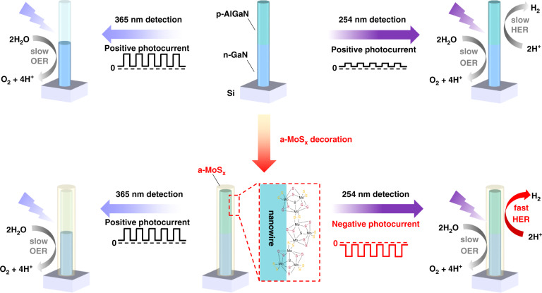
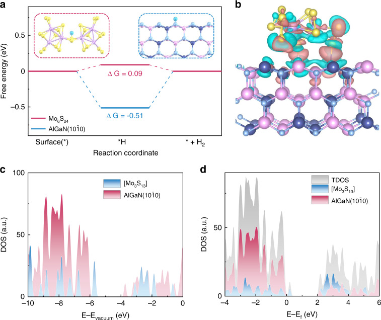
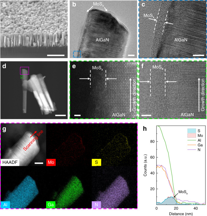
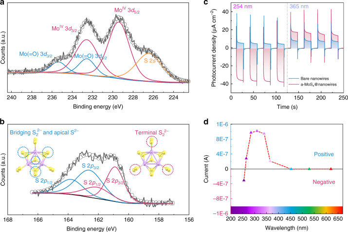
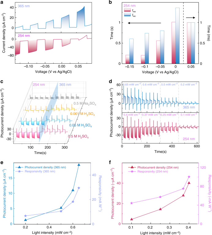
III-V semiconductor nanowires are indispensable building blocks for nanoscale electronic and optoelectronic devices. However, solely relying on their intrinsic physical and material properties sometimes limits device functionalities to meet the increasing demands in versatile and complex electronic world. By leveraging the distinctive nature of the one-dimensional geometry and large surface-to-volume ratio of the nanowires, new properties can be attained through monolithic integration of conventional nanowires with other easy-synthesized functional materials. Herein, we combine high-crystal-quality III-nitride nanowires with amorphous molybdenum sulfides (a-MoS) to construct III-nitride/a-MoS core-shell nanostructures. Upon light illumination, such nanostructures exhibit striking spectrally distinctive photodetection characteristic in photoelectrochemical environment, demonstrating a negative photoresponsivity of -100.42 mA W under 254 nm illumination, and a positive photoresponsivity of 29.5 mA W under 365 nm illumination. Density functional theory calculations reveal that the successful surface modification of the nanowires via a-MoS decoration accelerates the reaction process at the electrolyte/nanowire interface, leading to the generation of opposite photocurrent signals under different photon illumination. Most importantly, such polarity-switchable photoconductivity can be further tuned for multiple wavelength bands photodetection by simply adjusting the surrounding environment and/or tailoring the nanowire composition, showing great promise to build light-wavelength controllable sensing devices in the future.
III-V族半导体纳米线是纳米级电子和光电器件不可或缺的构建块。然而,仅仅依靠它们固有的物理和材料特性有时会限制器件功能,无法满足日益增长的通用和复杂电子世界的需求。通过利用纳米线一维几何结构的独特性质和大的表面积与体积比,可以通过将传统纳米线与其他易于合成的功能材料进行单片集成来获得新的特性。在此,我们将高质量晶体的III族氮化物纳米线与非晶态硫化钼(a-MoS)相结合,构建III族氮化物/a-MoS核壳纳米结构。在光照下,这种纳米结构在光电化学环境中表现出显著的光谱独特的光探测特性,在254nm光照下显示出-100.42 mA W的负光响应率,在365nm光照下显示出29.5 mA W的正光响应率。密度泛函理论计算表明,通过a-MoS修饰成功地对纳米线进行表面改性,加速了电解质/纳米线界面处的反应过程,导致在不同光子光照下产生相反的光电流信号。最重要的是,通过简单地调整周围环境和/或调整纳米线组成,可以进一步调整这种极性可切换的光电导率,以用于多波段光探测,这为未来构建光波长可控传感设备显示出巨大的潜力。