Ismail Walid, Ibrahim Ghada, Habib Mohamed A, Alduaij Omar K, Abdelfatah Mahmoud, El-Shaer Abdelhamid
Physics Department, Faculty of Science, Kafrelsheikh University, Kafrelsheikh 33516, Egypt.
Department of Chemistry, College of Science, Imam Mohammad Ibn Saud Islamic University (IMSIU), Riyadh 11623, Saudi Arabia.
Nanomaterials (Basel). 2023 May 30;13(11):1764. doi: 10.3390/nano13111764.
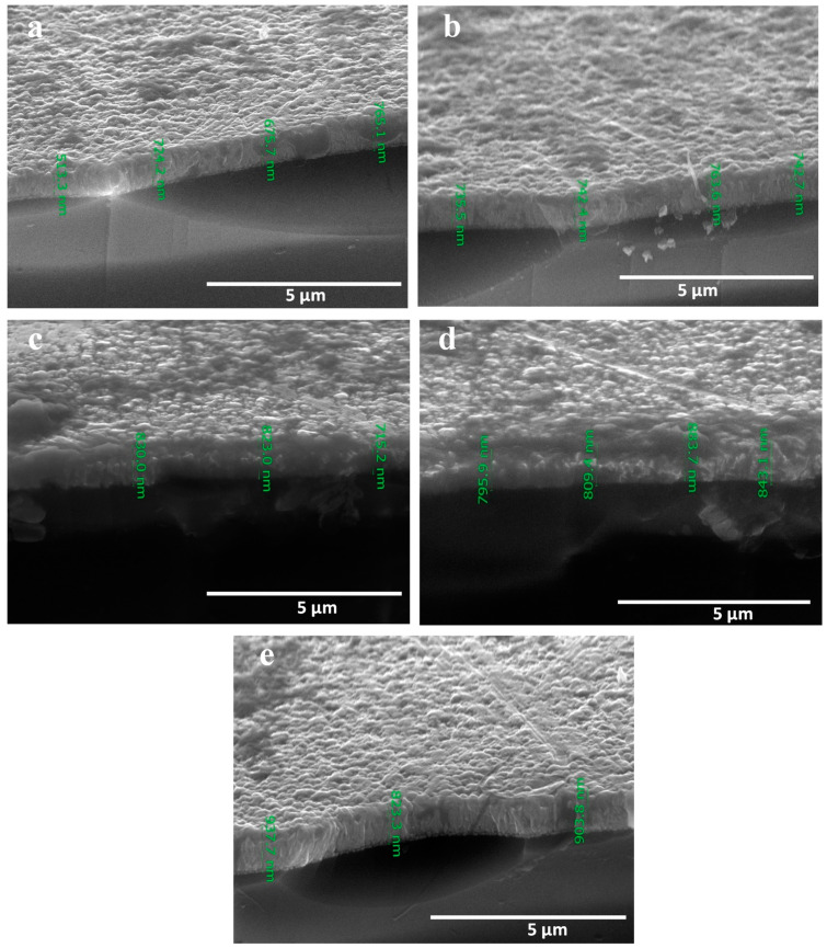
CdS thin films were grown on an FTO substrate at different temperatures, employing the low-cost hydrothermal method. All the fabricated CdS thin films were studied using XRD, Raman spectroscopy, SEM, PL spectroscopy, a UV-Vis spectrophotometer, photocurrent, Electrochemical Impedance Spectroscopy (EIS), and Mott-Schottky measurements. According to the XRD results, all the CdS thin films were formed in a cubic (zinc blende) structure with a favorable (111) orientation at various temperatures. The Scherrer equation was used to determine the crystal size of the CdS thin films, which varied from 25 to 40 nm. The SEM results indicated that the morphology of thin films seems to be dense, uniform, and tightly attached to the substrates. PL measurements showed the typical green and red emission peaks of CdS films at 520 nm and 705 nm, and these are attributable to free-carrier recombination and sulfur vacancies or cadmium vacancies, respectively. The optical absorption edge of the thin films was positioned between 500 and 517 nm which related to the CdS band gap. For the fabricated thin films, the estimated Eg was found to be between 2.50 and 2.39 eV. According to the photocurrent measurements, the CdS thin films grown were n-type semiconductors. As indicated by EIS, resistivity to charge transfer (RCT) decreased with temperature, reaching its lowest level at 250 °C. Flat band potential and donor density were found to fluctuate with temperature, from 0.39 to 0.76 V and 4.41 × 10 to 15.86 × 10 cm, respectively, according to Mott-Schottky measurements. Our results indicate that CdS thin films are promising candidates for optoelectronic applications.
采用低成本水热法在不同温度下于FTO衬底上生长硫化镉(CdS)薄膜。使用X射线衍射(XRD)、拉曼光谱、扫描电子显微镜(SEM)、光致发光(PL)光谱、紫外-可见分光光度计、光电流、电化学阻抗谱(EIS)和莫特-肖特基测量等方法对所有制备的CdS薄膜进行了研究。根据XRD结果,所有CdS薄膜在不同温度下均形成立方(闪锌矿)结构且具有良好的(111)取向。使用谢乐方程确定CdS薄膜的晶体尺寸,其范围为25至40纳米。SEM结果表明薄膜的形态似乎致密、均匀且紧密附着于衬底。PL测量显示CdS薄膜在520纳米和705纳米处有典型的绿色和红色发射峰,这些分别归因于自由载流子复合以及硫空位或镉空位。薄膜的光吸收边缘位于500至517纳米之间,这与CdS的带隙相关。对于制备的薄膜,估计的禁带宽度(Eg)在2.50至2.39电子伏特之间。根据光电流测量,生长的CdS薄膜为n型半导体。如EIS所示,电荷转移电阻(RCT)随温度降低,在250℃时达到最低水平。根据莫特-肖特基测量,发现平带电位和施主密度随温度波动,分别从0.39伏至0.76伏以及从4.41×10至15.86×10厘米。我们的结果表明CdS薄膜是光电子应用的有前途的候选材料。