Gianvittorio Stefano, Tonelli Domenica, Lesch Andreas
Department of Industrial Chemistry "Toso Montanari", University of Bologna, Center for Chemical Catalysis-C3, Viale del Risorgimento 4, 40136 Bologna, Italy.
Nanomaterials (Basel). 2023 Jun 23;13(13):1915. doi: 10.3390/nano13131915.
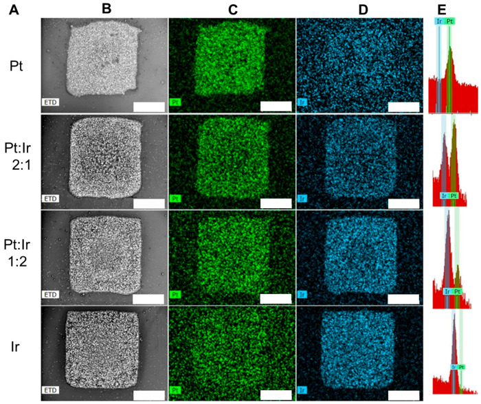
The fabrication of thin-film electrodes, which contain metal nanoparticles and nanostructures for applications in electrochemical sensing as well as energy conversion and storage, is often based on multi-step procedures that include two main passages: (i) the synthesis and purification of nanomaterials and (ii) the fabrication of thin films by coating electrode supports with these nanomaterials. The patterning and miniaturization of thin film electrodes generally require masks or advanced patterning instrumentation. In recent years, various approaches have been presented to integrate the spatially resolved deposition of metal precursor solutions and the rapid conversion of the precursors into metal nanoparticles. To achieve the latter, high intensity light irradiation has, in particular, become suitable as it enables the photochemical, photocatalytical, and photothermal conversion of the precursors during or slightly after the precursor deposition. The conversion of the metal precursors directly on the target substrates can make the use of capping and stabilizing agents obsolete. This review focuses on hybrid platforms that comprise digital metal precursor ink printing and high intensity light irradiation for inducing metal precursor conversions into patterned metal and alloy nanoparticles. The combination of the two methods has recently been named Print-Light-Synthesis by a group of collaborators and is characterized by its sustainability in terms of low material consumption, low material waste, and reduced synthesis steps. It provides high control of precursor loading and light irradiation, both affecting and improving the fabrication of thin film electrodes.
薄膜电极的制造涉及用于电化学传感以及能量转换和存储的金属纳米颗粒和纳米结构,其通常基于多步骤程序,包括两个主要步骤:(i)纳米材料的合成与纯化,以及(ii)通过用这些纳米材料涂覆电极载体来制造薄膜。薄膜电极的图案化和小型化通常需要掩膜或先进的图案化仪器。近年来,已经提出了各种方法来整合金属前驱体溶液的空间分辨沉积以及前驱体快速转化为金属纳米颗粒的过程。为了实现后者,高强度光照射尤其适用,因为它能够在前驱体沉积期间或之后不久实现前驱体的光化学、光催化和光热转化。金属前驱体在目标基板上直接转化可以使封端剂和稳定剂不再必要。本综述重点关注混合平台,该平台包括数字金属前驱体油墨印刷和高强度光照射,用于诱导金属前驱体转化为图案化的金属和合金纳米颗粒。一组合作者最近将这两种方法的结合命名为“打印 - 光合成”,其特点是在低材料消耗、低材料浪费和减少合成步骤方面具有可持续性。它提供了对前驱体负载和光照射的高度控制,这两者都影响并改善了薄膜电极的制造。