Altana Carmen, Calcagno Lucia, Ciampi Caterina, La Via Francesco, Lanzalone Gaetano, Muoio Annamaria, Pasquali Gabriele, Pellegrino Domenico, Puglia Sebastiana, Rapisarda Giuseppe, Tudisco Salvatore
Laboratori Nazionali del Sud (LNS), Istituto Nazionale di Fisica Nucleare (INFN), 95123 Catania, Italy.
Istituto Nazionale di Fisica Nucleare (INFN)-Sezione di Catania, 95123 Catania, Italy.
Sensors (Basel). 2023 Jul 19;23(14):6522. doi: 10.3390/s23146522.
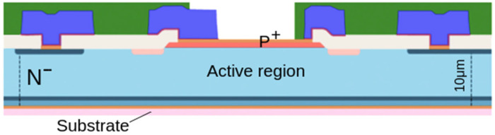
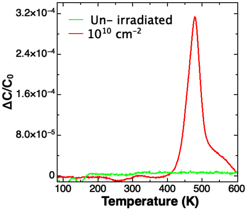
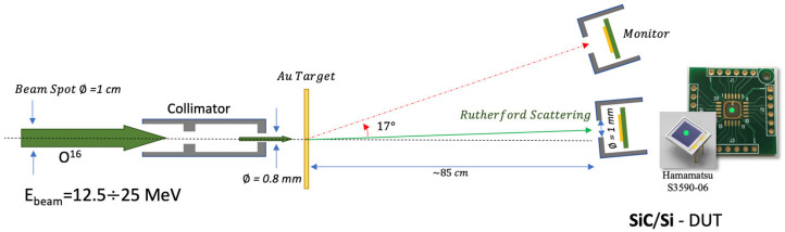
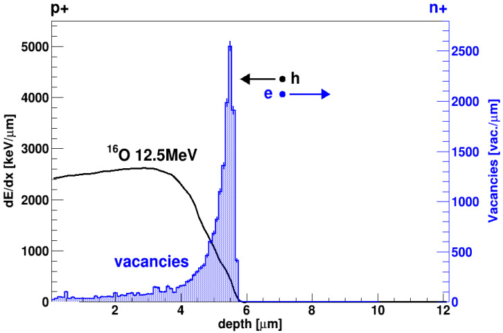
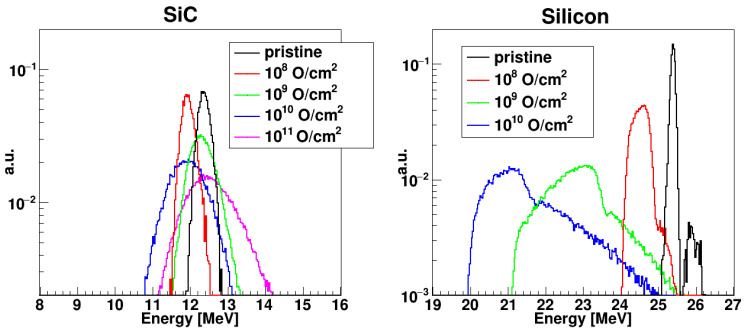
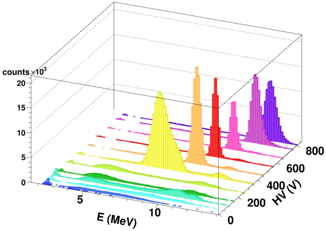
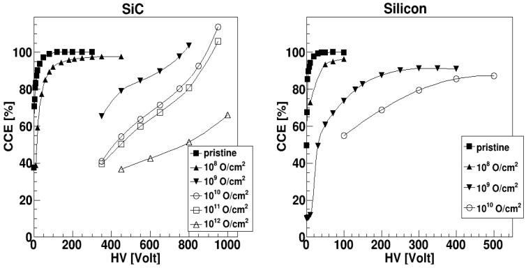
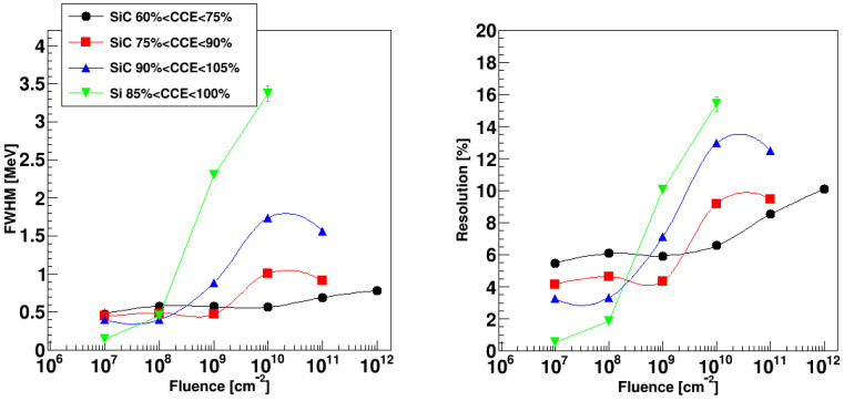
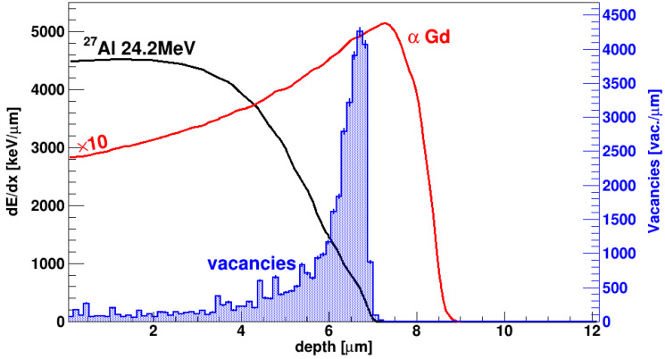
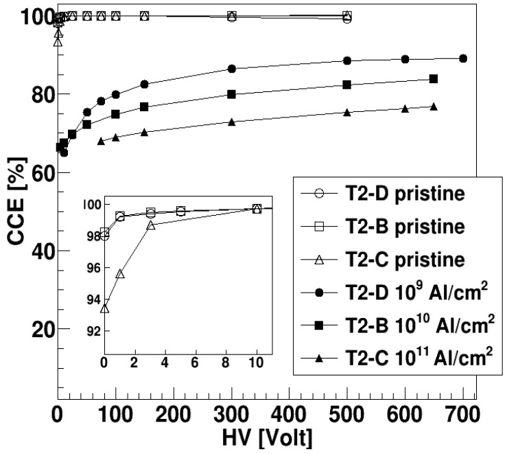
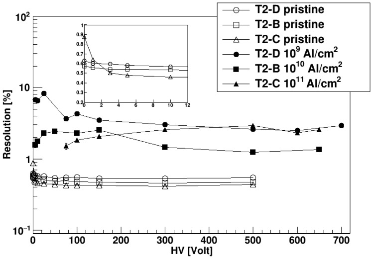
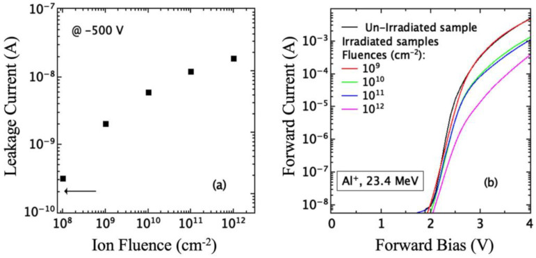
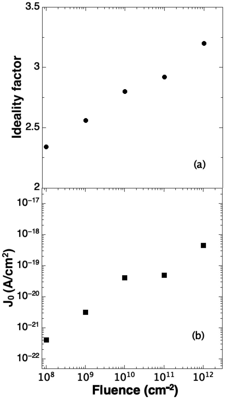
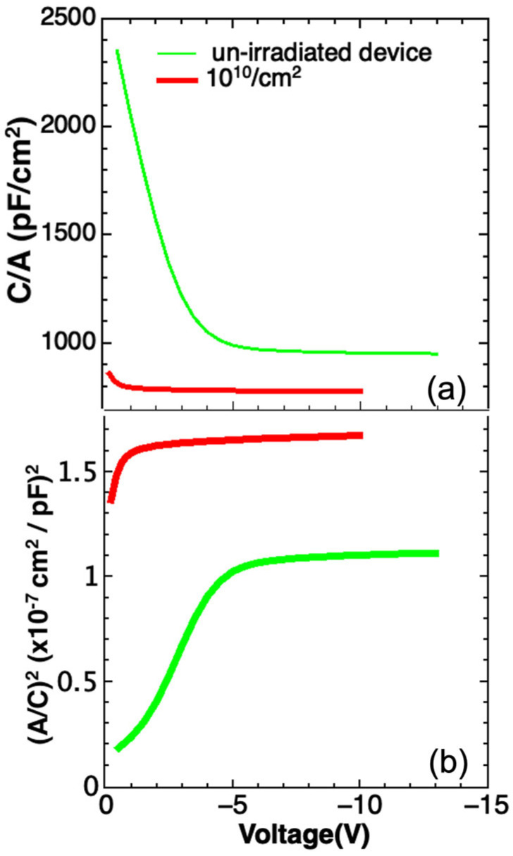
While silicon has been a steadfast semiconductor material for the past 50 years, it is now facing competition from other materials, especially for detector design. In that respect, due to its high resistance to radiation damage, silicon carbide is one of the most promising materials. In this work, we discuss the radiation damage studies of a new, large area, p-n junction silicon carbide device developed by the SiCILIA collaboration. We have studied the general performances of several devices, as a function of fluence, irradiated in different experimental conditions with different beams. A standard p-n junction silicon detector was also irradiated for comparison. The new detectors manifest excellent performance in terms of stability of the main parameters, linearity, defect distribution, charge collection efficiency, energy resolution, leakage current, etc. Experimental results evidence a radiation resistance of SiC devices more than two order of magnitude higher than Si devices. The new construction technology applied to silicon carbide material has made it possible to create very robust devices with excellent performance. These devices will soon be available for all those scientific projects where a high resistance to radiation damage is required.
在过去的50年里,硅一直是一种稳定的半导体材料,但现在它正面临来自其他材料的竞争,尤其是在探测器设计方面。在这方面,由于碳化硅对辐射损伤具有高抗性,它是最有前途的材料之一。在这项工作中,我们讨论了由SiCILIA合作开发的一种新型大面积p-n结碳化硅器件的辐射损伤研究。我们研究了几种器件在不同实验条件下用不同束流辐照时,其一般性能随注量的变化情况。还辐照了一个标准的p-n结硅探测器用于比较。新探测器在主要参数的稳定性、线性度、缺陷分布、电荷收集效率、能量分辨率、漏电流等方面表现出优异的性能。实验结果表明,碳化硅器件的抗辐射能力比硅器件高两个多数量级。应用于碳化硅材料的新制造技术使得制造出性能优异且非常坚固的器件成为可能。这些器件很快将可供所有那些需要高抗辐射损伤能力的科研项目使用。