Dyck Ondrej, Almutlaq Jawaher, Lingerfelt David, Swett Jacob L, Oxley Mark P, Huang Bevin, Lupini Andrew R, Englund Dirk, Jesse Stephen
Center for Nanophase Materials Sciences, Oak Ridge National Laboratory, Oak Ridge, TN, USA.
Massachusetts Institute of Technology, Cambridge, MA, USA.
Nat Commun. 2023 Nov 20;14(1):7550. doi: 10.1038/s41467-023-42256-9.
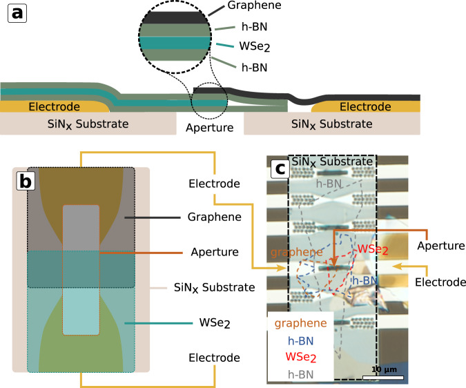
Recent studies of secondary electron (SE) emission in scanning transmission electron microscopes suggest that material's properties such as electrical conductivity, connectivity, and work function can be probed with atomic scale resolution using a technique known as secondary electron e-beam-induced current (SEEBIC). Here, we apply the SEEBIC imaging technique to a stacked 2D heterostructure device to reveal the spatially resolved electron density of an encapsulated WSe layer. We find that the double Se lattice site shows higher emission than the W site, which is at odds with first-principles modelling of valence ionization of an isolated WSe cluster. These results illustrate that atomic level SEEBIC contrast within a single material is possible and that an enhanced understanding of atomic scale SE emission is required to account for the observed contrast. In turn, this suggests that, in the future, subtle information about interlayer bonding and the effect on electron orbitals could be directly revealed with this technique.
近期对扫描透射电子显微镜中二次电子(SE)发射的研究表明,使用一种称为二次电子电子束诱导电流(SEEBIC)的技术,可以在原子尺度分辨率下探测材料的诸如电导率、连通性和功函数等性质。在此,我们将SEEBIC成像技术应用于堆叠的二维异质结构器件,以揭示封装的WSe层的空间分辨电子密度。我们发现,双硒晶格位点的发射比钨位点更高,这与孤立WSe簇价态电离的第一性原理模型不一致。这些结果表明,在单一材料内实现原子级SEEBIC对比度是可能的,并且需要增强对原子尺度SE发射的理解来解释观察到的对比度。反过来,这表明,未来可以用该技术直接揭示有关层间键合和对电子轨道影响的细微信息。