Chen Jingjing, Su Xujun, Wang Guobing, Niu Mutong, Li Xinran, Xu Ke
Suzhou Institute of Nano-tech and Nano-bionics, CAS, Ruoshui Road 398, Suzhou Industrial Park, Suzhou, 215123, China.
Shenyang National Laboratory for Materials Science, Jiangsu Institute of Advanced Semiconductors, Suzhou, 215123, China.
Discov Nano. 2024 Mar 7;19(1):40. doi: 10.1186/s11671-024-03983-0.
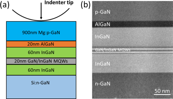
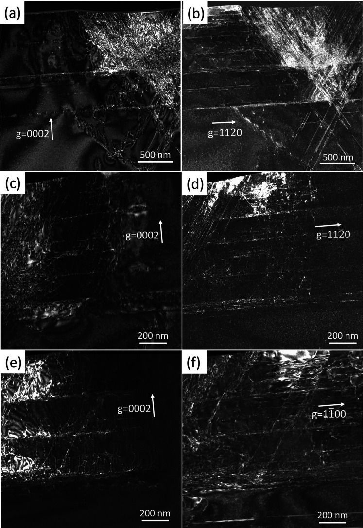
The slip systems and motion behavior of dislocations induced by nano-indentation technique in GaN-based LDs were investigated. Dislocations with burgers vector of b = 1/3 <11 3> were introduced on either {11 2} <11 3>, or {1 01} <11 3> pyramidal slip systems in the upper p-GaN layer. Besides, {0001} <11 0> basal slip system was also activated. The AlGaN/InGaN multi-layers in device can provide mismatch stresses to prevent dislocations from slipping through. It was observed that the density of dislocations induced by the indenter significantly decreased from the upper to the lower regions of the multi-layers. The a + c dislocations on pyramidal slip planes were mostly blocked by the strained layers.
研究了基于GaN的发光二极管中通过纳米压痕技术诱导的位错滑移系统和运动行为。在顶部p-GaN层的{11 2}<11 3>或{1 01}<11 3>金字塔形滑移系统上引入了柏氏矢量b = 1/3<11 3>的位错。此外,{0001}<11 0>基面滑移系统也被激活。器件中的AlGaN/InGaN多层结构可以提供失配应力,以防止位错滑移通过。观察到由压头诱导的位错密度从多层结构的上部到下部区域显著降低。金字塔形滑移面上的a + c位错大多被应变层阻挡。