School of Power and Mechanical Engineering, Wuhan University, Wuhan, 430072, China.
Quantum Wafer Inc., Foshan, 528251, China.
Sci Rep. 2017 Mar 15;7:44627. doi: 10.1038/srep44627.
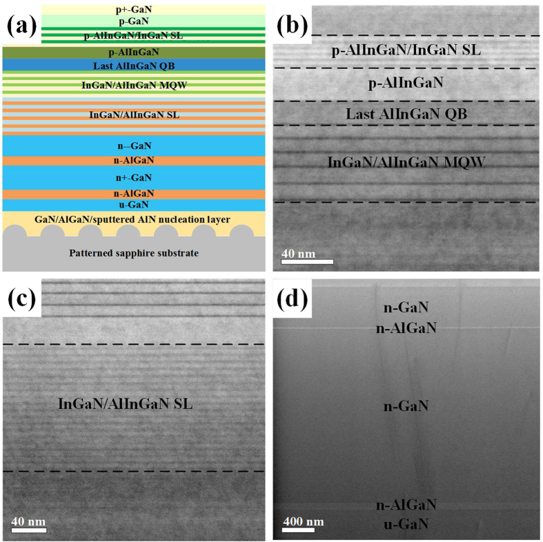
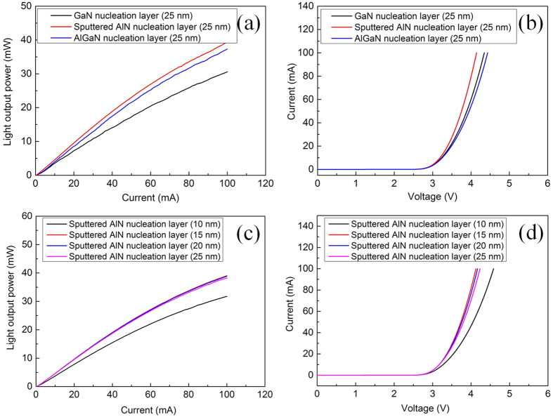
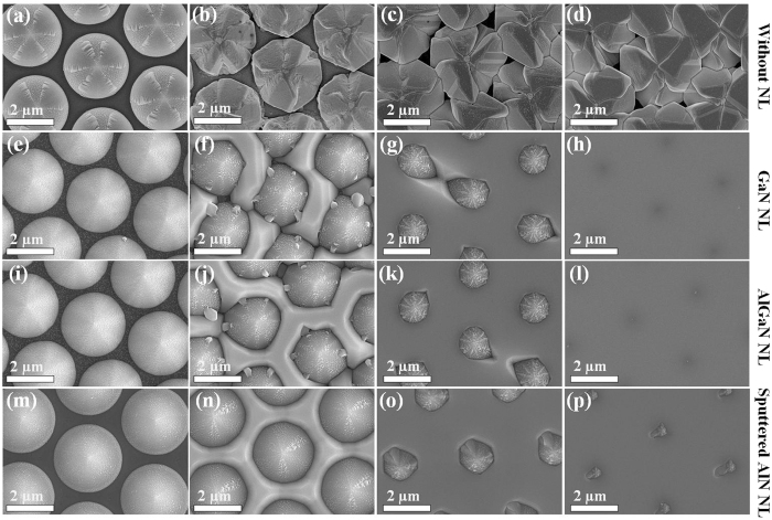
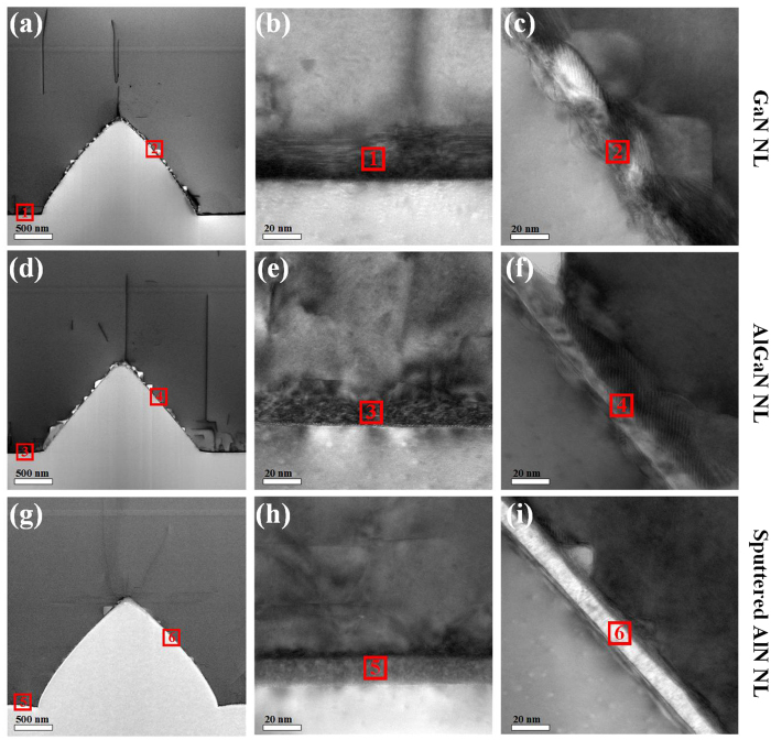
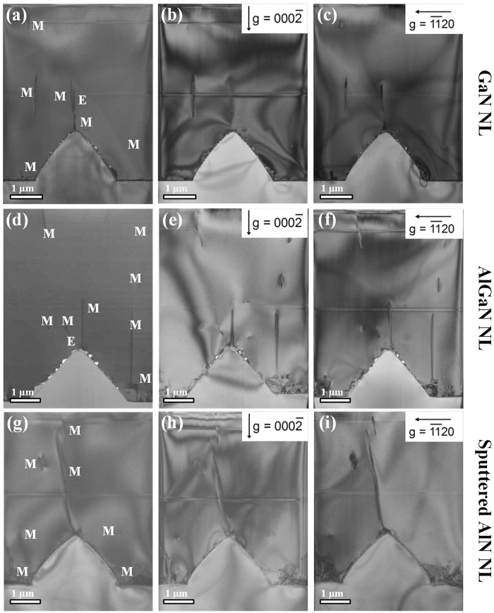
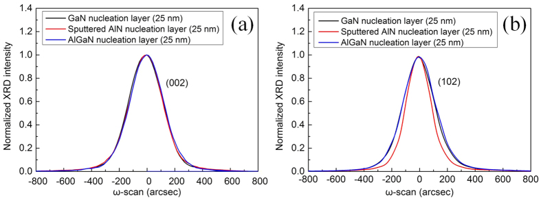
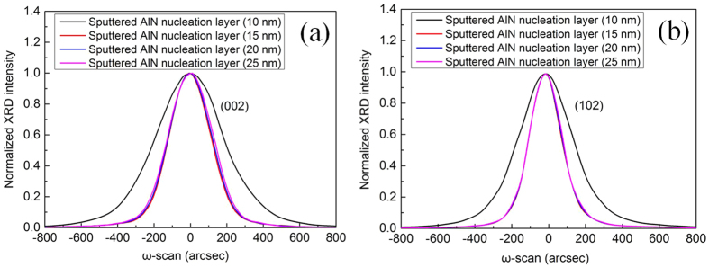
We report on the demonstration of GaN-based ultraviolet light-emitting diodes (UV LEDs) emitting at 375 nm grown on patterned sapphire substrate (PSS) with in-situ low temperature GaN/AlGaN nucleation layers (NLs) and ex-situ sputtered AlN NL. The threading dislocation (TD) densities in GaN-based UV LEDs with GaN/AlGaN/sputtered AlN NLs were determined by high-resolution X-ray diffraction (XRD) and cross-sectional transmission electron microscopy (TEM), which revealed that the TD density in UV LED with AlGaN NL was the highest, whereas that in UV LED with sputtered AlN NL was the lowest. The light output power (LOP) of UV LED with AlGaN NL was 18.2% higher than that of UV LED with GaN NL owing to a decrease in the absorption of 375 nm UV light in the AlGaN NL with a larger bandgap. Using a sputtered AlN NL instead of the AlGaN NL, the LOP of UV LED was further enhanced by 11.3%, which is attributed to reduced TD density in InGaN/AlInGaN active region. In the sputtered AlN thickness range of 10-25 nm, the LOP of UV LED with 15-nm-thick sputtered AlN NL was the highest, revealing that optimum thickness of the sputtered AlN NL is around 15 nm.
我们展示了在具有原位低温 GaN/AlGaN 成核层 (NL) 和外延溅射 AlN NL 的图案化蓝宝石衬底 (PSS) 上生长的 GaN 基 375nm 紫外发光二极管 (UV LED)。通过高分辨率 X 射线衍射 (XRD) 和横截面透射电子显微镜 (TEM) 确定了具有 GaN/AlGaN/溅射 AlN NL 的 GaN 基 UV LED 的位错密度,结果表明具有 AlGaN NL 的 UV LED 的位错密度最高,而具有溅射 AlN NL 的 UV LED 的位错密度最低。由于具有较大能带隙的 AlGaN NL 中 375nm UV 光的吸收减少,具有 AlGaN NL 的 UV LED 的光输出功率 (LOP) 比具有 GaN NL 的 UV LED 高 18.2%。使用溅射 AlN NL 代替 AlGaN NL,UV LED 的 LOP 进一步提高了 11.3%,这归因于 InGaN/AlInGaN 有源区中的位错密度降低。在溅射 AlN 厚度范围为 10-25nm 时,具有 15nm 厚溅射 AlN NL 的 UV LED 的 LOP 最高,表明溅射 AlN NL 的最佳厚度约为 15nm。