Wang Huawei, Bai Pengfei, Cui He, Zhang Xiaotong, Tang Yifan, Liang Shaoyu, Li Shixiao, Zhou Guofu
Guangdong Provincial Key Laboratory of Optical Information Materials and Technology & Institute of Electronic Paper Displays, South China Academy of Advanced Optoelectronics, South China Normal University, Guangzhou, 510006, PR China.
Shenzhen Guohua Optoelectronics Tech. Co., Ltd., Shenzhen, 518110, PR China.
Commun Eng. 2025 Jan 4;4(1):1. doi: 10.1038/s44172-024-00338-6.
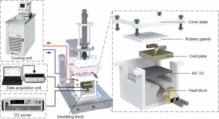
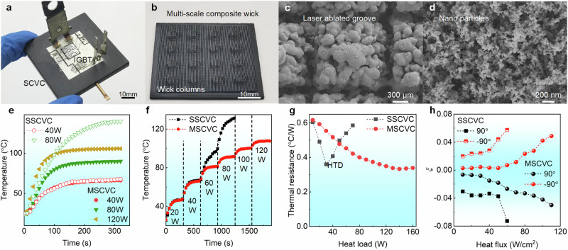
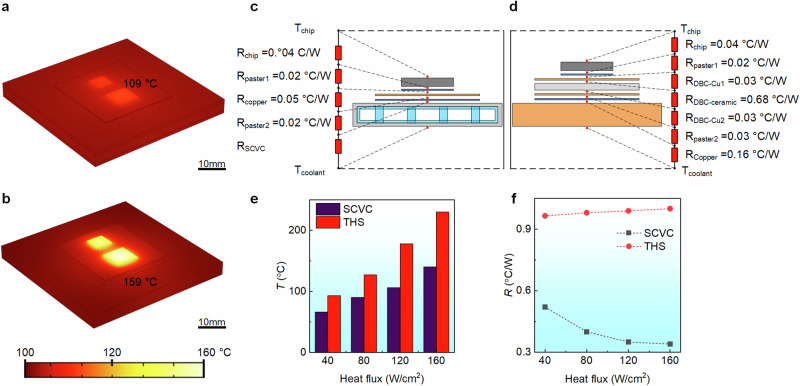
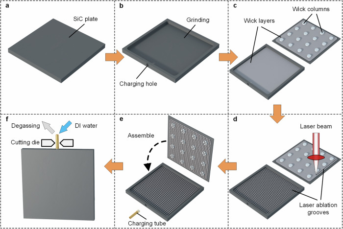
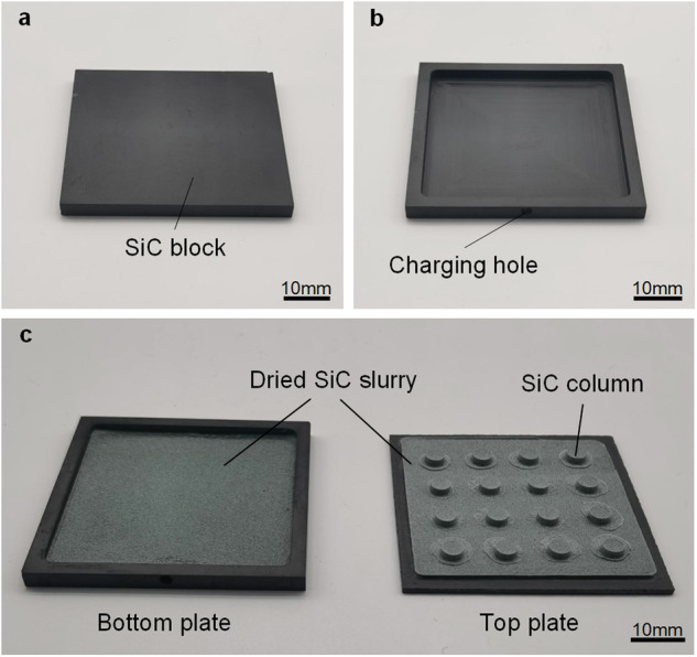
Conventional electronic chip packaging generates a huge thermal resistance due to the low thermal conductivity of the packaging materials that separate chip dies and coolant. Here we propose and fabricate a closed high-conducting heat chip package based on passive phase change, using silicon carbide which is physically and structurally compatible with chip die materials. Our "chip on vapor chamber" (CoVC) concept realizes rapid diffusion of hot spots, and eliminates the high energy consumption of refrigeration ordinarily required for heat management. Multi-scale wicks and bionic vein structures are applied to CoVC leading to an increase of 164% in heat transfer performance. The thermal resistance of the package was only a third that of traditional packaging systems. This means that the structure of CoVC has a good thermal conducting ability and can reduce energy consumption for heat dissipation.
传统的电子芯片封装由于分隔芯片管芯和冷却剂的封装材料的低导热率而产生巨大的热阻。在此,我们提出并制造了一种基于被动相变的封闭高导热芯片封装,使用与芯片管芯材料在物理和结构上兼容的碳化硅。我们的“芯片置于汽相室”(CoVC)概念实现了热点的快速扩散,并消除了通常用于热管理的制冷的高能耗。多尺度芯吸结构和仿生静脉结构应用于CoVC,使传热性能提高了164%。该封装的热阻仅为传统封装系统的三分之一。这意味着CoVC结构具有良好的导热能力,并且可以降低散热的能量消耗。