Crisci Teresa, Moretti Luigi, Gioffrè Mariano, Hashemi Babak, Mammeri Mohamed, Della Corte Francesco Giuseppe, Casalino Maurizio
Department of Electrical Engineering and Information Technology, University of Naples Federico II, Via Claudio 21, 80125 Napoli, Italy.
Institute of Applied Science and Intelligent Systems "Eduardo Caianiello" (CNR), Via P. Castellino n. 141, 800131 Naples, Italy.
Micromachines (Basel). 2025 Apr 8;16(4):440. doi: 10.3390/mi16040440.
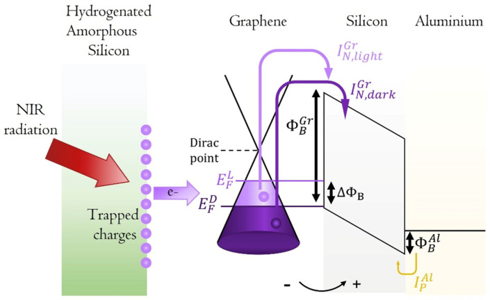
In this work, we present a graphene-based photodetector operating at a wavelength of 1310 nm. The device leverages the SPARK effect, which has previously been investigated only at 1550 nm. It features a hybrid waveguide structure comprising hydrogenated amorphous silicon, graphene, and crystalline silicon. Upon optical illumination, defect states release charge carriers into the graphene layer, modulating the thermionic current across the graphene/crystalline silicon Schottky junction. The photodetector demonstrates a peak responsivity of 0.3 A/W at 1310 nm, corresponding to a noise-equivalent power of 0.4 pW/Hz. The experimental results provide deeper insights into the SPARK effect by enabling the determination of the efficiency × lifetime product of carriers at 1310 nm and its comparison with values previously reported at 1550 nm. The wavelength dependence of this product is analyzed and discussed. Additionally, the response times of the device are measured and evaluated. The silicon-based fabrication approach employed is versatile and does not rely on sub-micron lithography techniques. Notably, reducing the incident optical power enhances the responsivity, making this photodetector highly suitable for power monitoring applications in integrated photonic circuits.
在这项工作中,我们展示了一种工作波长为1310 nm的基于石墨烯的光电探测器。该器件利用了SPARK效应,此前该效应仅在1550 nm波长下进行过研究。它具有一种混合波导结构,由氢化非晶硅、石墨烯和晶体硅组成。在光照射下,缺陷态将电荷载流子释放到石墨烯层中,调制穿过石墨烯/晶体硅肖特基结的热电子电流。该光电探测器在1310 nm处的峰值响应率为0.3 A/W,对应的噪声等效功率为0.4 pW/Hz。实验结果通过确定1310 nm处载流子的效率×寿命乘积并将其与先前在1550 nm处报道的值进行比较,为SPARK效应提供了更深入的见解。分析并讨论了该乘积的波长依赖性。此外,还对器件的响应时间进行了测量和评估。所采用的基于硅的制造方法具有通用性,不依赖于亚微米光刻技术。值得注意的是,降低入射光功率会提高响应率,这使得该光电探测器非常适合集成光子电路中的功率监测应用。