School of Materials Science and Engineering, Key Laboratory of Advanced Materials, Tsinghua University, Beijing 100084, People's Republic of China.
Nanoscale Res Lett. 2013 Oct 1;8(1):405. doi: 10.1186/1556-276X-8-405.
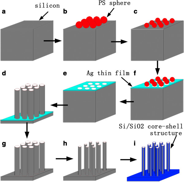
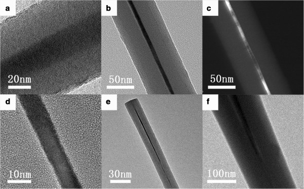
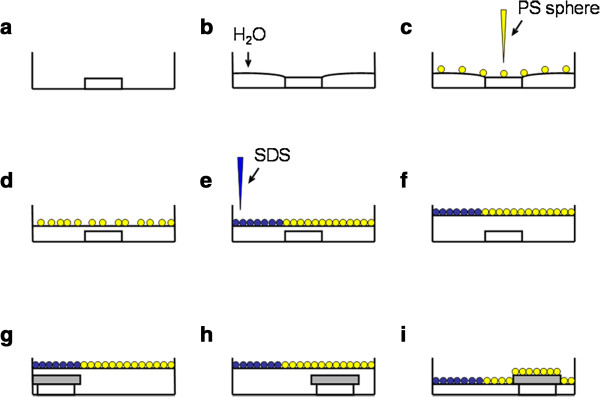
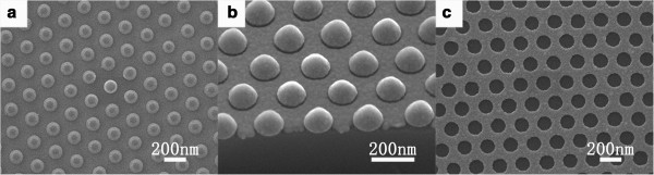
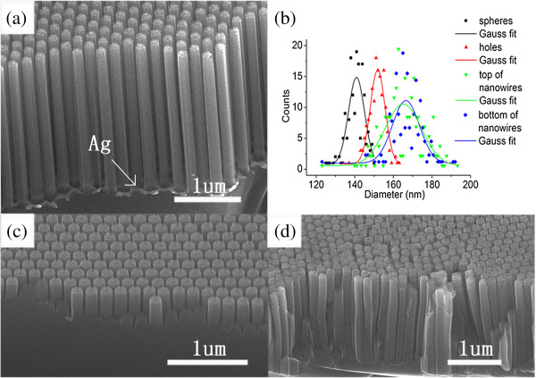
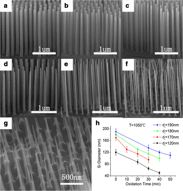
A combination of template-assisted metal catalytic etching and self-limiting oxidation has been successfully implemented to yield core-shell silicon nanowire arrays with inner diameter down to sub-10 nm. The diameter of the polystyrene spheres after reactive ion etching and the thickness of the deposited Ag film are both crucial for the removal of the polystyrene spheres. The mean diameter of the reactive ion-etched spheres, the holes on the Ag film, and the nanowires after metal catalytic etching exhibit an increasing trend during the synthesis process. Two-step dry oxidation and post-chemical etching were employed to reduce the diameter of the silicon nanowires to approximately 50 nm. A self-limiting effect was induced by further oxidation at lower temperatures (750°C ~ 850°C), and core-shell silicon nanowire arrays with controllable diameter were obtained.
采用模板辅助金属催化刻蚀和自限制氧化相结合的方法,成功地制备了内直径低至亚 10nm 的核壳硅纳米线阵列。反应离子刻蚀后聚苯乙烯球的直径和沉积的 Ag 膜的厚度对于去除聚苯乙烯球都至关重要。在合成过程中,反应离子刻蚀后的球、Ag 膜上的孔和金属催化刻蚀后的纳米线的平均直径都呈现出增大的趋势。采用两步干法氧化和后化学刻蚀将硅纳米线的直径减小到约 50nm。在较低温度(750°C~850°C)下进一步氧化诱导了自限制效应,得到了具有可控直径的核壳硅纳米线阵列。