• 文献检索
  • 文档翻译
  • 深度研究
  • 学术资讯
  • Suppr Zotero 插件Zotero 插件
  • 邀请有礼
  • 套餐&价格
  • 历史记录
应用&插件
Suppr Zotero 插件Zotero 插件浏览器插件Mac 客户端Windows 客户端微信小程序
定价
高级版会员购买积分包购买API积分包
服务
文献检索文档翻译深度研究API 文档MCP 服务
关于我们
关于 Suppr公司介绍联系我们用户协议隐私条款
关注我们

Suppr 超能文献

核心技术专利:CN118964589B侵权必究
粤ICP备2023148730 号-1Suppr @ 2026

文献检索

告别复杂PubMed语法,用中文像聊天一样搜索,搜遍4000万医学文献。AI智能推荐,让科研检索更轻松。

立即免费搜索

文件翻译

保留排版,准确专业,支持PDF/Word/PPT等文件格式,支持 12+语言互译。

免费翻译文档

深度研究

AI帮你快速写综述,25分钟生成高质量综述,智能提取关键信息,辅助科研写作。

立即免费体验

沉积在介电衬底上的MoS₂薄膜中自然电子掺杂的光学研究。

Optical investigation of the natural electron doping in thin MoS2 films deposited on dielectric substrates.

作者信息

Sercombe D, Schwarz S, Del Pozo-Zamudio O, Liu F, Robinson B J, Chekhovich E A, Tartakovskii I I, Kolosov O, Tartakovskii A I

机构信息

Department of Physics and Astronomy, University of Sheffield, Sheffield S3 7RH, United Kingdom.

1] Department of Physics and Astronomy, University of Sheffield, Sheffield S3 7RH, United Kingdom [2] Experimentelle Physik 2, Technische Universität Dortmund, 44221 Dortmund, Germany.

出版信息

Sci Rep. 2013 Dec 12;3:3489. doi: 10.1038/srep03489.

DOI:10.1038/srep03489
PMID:24336152
原文链接:https://pmc.ncbi.nlm.nih.gov/articles/PMC3860010/
Abstract

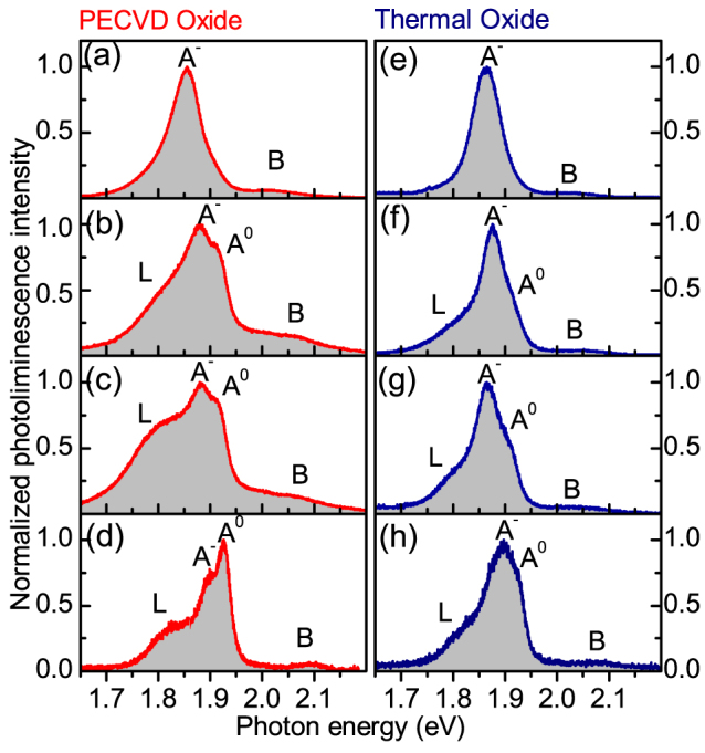
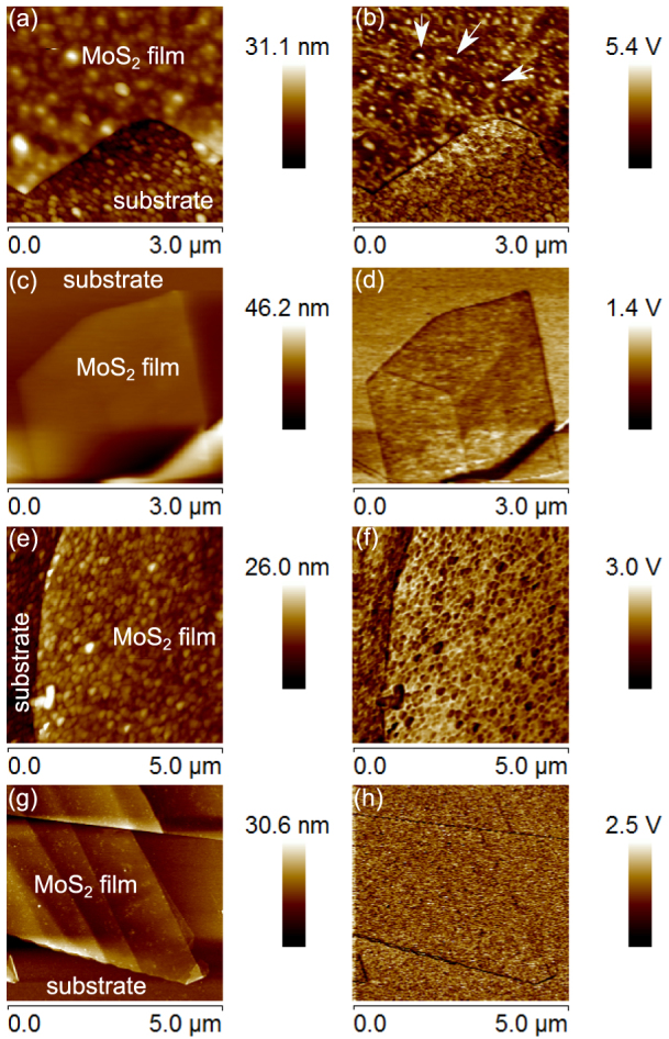
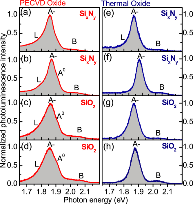
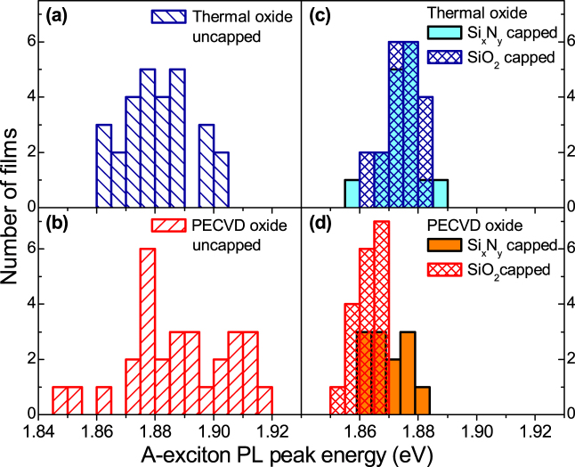
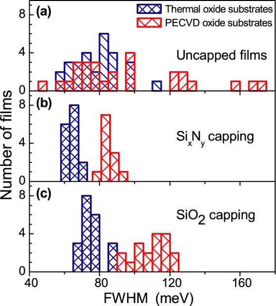
Two-dimensional (2D) compounds provide unique building blocks for novel layered devices and hybrid photonic structures. However, large surface-to-volume ratio in thin films enhances the significance of surface interactions and charging effects requiring new understanding. Here we use micro-photoluminescence (PL) and ultrasonic force microscopy to explore the influence of the dielectric environment on optical properties of a few monolayer MoS2 films. PL spectra for MoS2 films deposited on SiO2 substrates are found to vary widely. This film-to-film variation is suppressed by additional capping of MoS2 with SiO2 and Si(x)N(y), improving mechanical coupling of MoS2 with surrounding dielectrics. We show that the observed PL non-uniformities are related to strong variation in the local electron charging of MoS2 films. In completely encapsulated films, negative charging is enhanced leading to uniform optical properties. Observed great sensitivity of optical characteristics of 2D films to surface interactions has important implications for optoelectronics applications of layered materials.

摘要

二维(2D)化合物为新型层状器件和混合光子结构提供了独特的构建块。然而,薄膜中较大的表面积与体积比增强了表面相互作用和电荷效应的重要性,这需要新的理解。在这里,我们使用微光致发光(PL)和超声力显微镜来探索介电环境对几层单层二硫化钼(MoS2)薄膜光学性质的影响。发现沉积在二氧化硅(SiO2)衬底上的MoS2薄膜的PL光谱变化很大。通过用SiO2和Si(x)N(y)对MoS2进行额外的覆盖,这种薄膜间的变化得到了抑制,改善了MoS2与周围电介质的机械耦合。我们表明,观察到的PL不均匀性与MoS2薄膜局部电子充电的强烈变化有关。在完全封装的薄膜中,负电荷增强,导致光学性质均匀。观察到二维薄膜的光学特性对表面相互作用具有极大的敏感性,这对层状材料的光电子应用具有重要意义。

https://cdn.ncbi.nlm.nih.gov/pmc/blobs/0058/3860010/658fbdf0c9fb/srep03489-f5.jpg
https://cdn.ncbi.nlm.nih.gov/pmc/blobs/0058/3860010/301a00c2c5f3/srep03489-f1.jpg
https://cdn.ncbi.nlm.nih.gov/pmc/blobs/0058/3860010/b90006934213/srep03489-f2.jpg
https://cdn.ncbi.nlm.nih.gov/pmc/blobs/0058/3860010/95a867232273/srep03489-f3.jpg
https://cdn.ncbi.nlm.nih.gov/pmc/blobs/0058/3860010/025a1112c52f/srep03489-f4.jpg
https://cdn.ncbi.nlm.nih.gov/pmc/blobs/0058/3860010/658fbdf0c9fb/srep03489-f5.jpg

相似文献

1
Optical investigation of the natural electron doping in thin MoS2 films deposited on dielectric substrates.沉积在介电衬底上的MoS₂薄膜中自然电子掺杂的光学研究。
Sci Rep. 2013 Dec 12;3:3489. doi: 10.1038/srep03489.
2
Controlled Gas Molecules Doping of Monolayer MoS via Atomic-Layer-Deposited AlO Films.通过原子层沉积 AlO 薄膜对单层 MoS 进行受控气体分子掺杂。
ACS Appl Mater Interfaces. 2017 Aug 23;9(33):27402-27408. doi: 10.1021/acsami.7b08893. Epub 2017 Aug 15.
3
Improving the Photoelectric Characteristics of MoS Thin Films by Doping Rare Earth Element Erbium.通过掺杂稀土元素铒改善二硫化钼薄膜的光电特性
Nanoscale Res Lett. 2016 Dec;11(1):513. doi: 10.1186/s11671-016-1729-6. Epub 2016 Nov 22.
4
Scanning Near-Field Optical Microscopy of Ultrathin Gold Films.超薄金膜的扫描近场光学显微镜
Nanomaterials (Basel). 2023 Apr 15;13(8):1376. doi: 10.3390/nano13081376.
5
Probing the Optical Properties of MoS on SiO/Si and Sapphire Substrates.探究在SiO/Si和蓝宝石衬底上的二硫化钼的光学性质。
Nanomaterials (Basel). 2019 May 14;9(5):740. doi: 10.3390/nano9050740.
6
Microscopic evidence of strong interactions between chemical vapor deposited 2D MoS film and SiO growth template.化学气相沉积二维MoS薄膜与SiO生长模板之间强相互作用的微观证据。
Nano Converg. 2021 Apr 9;8(1):11. doi: 10.1186/s40580-021-00262-x.
7
Reversible photoluminescence modulation of monolayer MoS on a ferroelectric substrate by light irradiation and thermal annealing.通过光照射和热退火对铁电衬底上的单层二硫化钼进行可逆光致发光调制。
Phys Chem Chem Phys. 2021 Aug 28;23(32):17265-17270. doi: 10.1039/d1cp02248b. Epub 2021 Aug 4.
8
Role of Hole Trap Sites in MoS for Inconsistency in Optical and Electrical Phenomena.MoS 中孔陷阱位在光学和电学现象不一致中的作用。
ACS Appl Mater Interfaces. 2018 Mar 28;10(12):10580-10586. doi: 10.1021/acsami.8b00541. Epub 2018 Mar 13.
9
Combinatorial Large-Area MoS/Anatase-TiO Interface: A Pathway to Emergent Optical and Optoelectronic Functionalities.组合大面积MoS/锐钛矿型TiO界面:通往新兴光学和光电功能的途径。
ACS Appl Mater Interfaces. 2020 Sep 30;12(39):44345-44359. doi: 10.1021/acsami.0c13342. Epub 2020 Sep 17.
10
Sub-10 nm Tunable Hybrid Dielectric Engineering on MoS for Two-Dimensional Material-Based Devices.亚 10nm 可调谐混合介电工程在 MoS 上的二维材料基器件
ACS Nano. 2017 Oct 24;11(10):10243-10252. doi: 10.1021/acsnano.7b04813. Epub 2017 Aug 30.

引用本文的文献

1
Interface analysis of oxide free MoS films fabricated by solution process.溶液法制备的无氧化物MoS薄膜的界面分析
Sci Rep. 2024 Nov 5;14(1):26779. doi: 10.1038/s41598-024-78229-1.
2
Long lived photogenerated charge carriers in few-layer transition metal dichalcogenides obtained from liquid phase exfoliation.通过液相剥离法获得的少层过渡金属二硫属化物中的长寿命光生电荷载流子。
Nanoscale Adv. 2023 Nov 29;6(4):1074-1083. doi: 10.1039/d3na00862b. eCollection 2024 Feb 13.
3
The Characteristics of the Metal-Free and Non-Conjugated Polymer Film with Self-Assembled Nanoparticles.

本文引用的文献

1
Local strain engineering in atomically thin MoS2.原子层厚 MoS2 的局域应变工程。
Nano Lett. 2013;13(11):5361-6. doi: 10.1021/nl402875m. Epub 2013 Oct 3.
2
Bandgap engineering of strained monolayer and bilayer MoS2.应变单层和双层 MoS2 的能带工程。
Nano Lett. 2013 Aug 14;13(8):3626-30. doi: 10.1021/nl4014748. Epub 2013 Jul 9.
3
Experimental demonstration of continuous electronic structure tuning via strain in atomically thin MoS2.通过原子级薄 MoS2 中的应变实现连续电子结构调控的实验演示。
具有自组装纳米颗粒的无金属非共轭聚合物薄膜的特性
Nanomaterials (Basel). 2023 Feb 2;13(3):596. doi: 10.3390/nano13030596.
4
The Optical Properties of Metal-Free Polymer Films with Self-Assembled Nanoparticles.具有自组装纳米粒子的无金属聚合物薄膜的光学性质
Polymers (Basel). 2021 Dec 2;13(23):4230. doi: 10.3390/polym13234230.
5
Enhancing and controlling valley magnetic response in MoS/WS heterostructures by all-optical route.通过全光途径增强和控制MoS/WS异质结构中的谷磁响应。
Nat Commun. 2019 Sep 17;10(1):4226. doi: 10.1038/s41467-019-12128-2.
6
Interlayer Difference of Bilayer-Stacked MoS Structure: Probing by Photoluminescence and Raman Spectroscopy.双层堆叠MoS结构的层间差异:通过光致发光和拉曼光谱进行探测
Nanomaterials (Basel). 2019 May 24;9(5):796. doi: 10.3390/nano9050796.
7
Photonic-crystal exciton-polaritons in monolayer semiconductors.单层半导体中的光子晶体激子极化激元。
Nat Commun. 2018 Feb 19;9(1):713. doi: 10.1038/s41467-018-03188-x.
8
Structural phase transition in monolayer MoTe driven by electrostatic doping.由静电掺杂驱动的单层 MoTe2 的结构相变。
Nature. 2017 Oct 26;550(7677):487-491. doi: 10.1038/nature24043. Epub 2017 Oct 11.
9
Direct exciton emission from atomically thin transition metal dichalcogenide heterostructures near the lifetime limit.来自接近寿命极限的原子级薄过渡金属二硫属化物异质结构的直接激子发射。
Sci Rep. 2017 Sep 28;7(1):12383. doi: 10.1038/s41598-017-09739-4.
10
Direct and Scalable Deposition of Atomically Thin Low-Noise MoS2 Membranes on Apertures.在孔径上直接且可扩展地沉积原子级薄的低噪声二硫化钼薄膜。
ACS Nano. 2015 Jul 28;9(7):7352-9. doi: 10.1021/acsnano.5b02369. Epub 2015 Jun 30.
Nano Lett. 2013 Jun 12;13(6):2931-6. doi: 10.1021/nl4013166. Epub 2013 May 17.
4
Electroluminescence in single layer MoS2.单层 MoS2 的电致发光。
Nano Lett. 2013 Apr 10;13(4):1416-21. doi: 10.1021/nl400516a. Epub 2013 Mar 29.
5
Tightly bound trions in monolayer MoS2.单层 MoS2 中的束缚紧密的三电子空穴。
Nat Mater. 2013 Mar;12(3):207-11. doi: 10.1038/nmat3505. Epub 2012 Dec 2.
6
Electronics and optoelectronics of two-dimensional transition metal dichalcogenides.二维过渡金属二卤族化合物的电子学和光电学。
Nat Nanotechnol. 2012 Nov;7(11):699-712. doi: 10.1038/nnano.2012.193.
7
Coupled spin and valley physics in monolayers of MoS2 and other group-VI dichalcogenides.MoS2 和其他 VI 族二维半导体单层中的耦合自旋和谷物理。
Phys Rev Lett. 2012 May 11;108(19):196802. doi: 10.1103/PhysRevLett.108.196802. Epub 2012 May 7.
8
Valley polarization in MoS2 monolayers by optical pumping.光学泵浦诱导 MoS2 单层中的谷极化。
Nat Nanotechnol. 2012 Aug;7(8):490-3. doi: 10.1038/nnano.2012.95. Epub 2012 Jun 17.
9
Control of valley polarization in monolayer MoS2 by optical helicity.通过光学螺旋控制单层 MoS2 中的谷极化。
Nat Nanotechnol. 2012 Aug;7(8):494-8. doi: 10.1038/nnano.2012.96. Epub 2012 Jun 17.
10
Valley-selective circular dichroism of monolayer molybdenum disulphide.单层二硫化钼的谷选择圆二色性。
Nat Commun. 2012 Jun 6;3:887. doi: 10.1038/ncomms1882.