• 文献检索
  • 文档翻译
  • 深度研究
  • 学术资讯
  • Suppr Zotero 插件Zotero 插件
  • 邀请有礼
  • 套餐&价格
  • 历史记录
应用&插件
Suppr Zotero 插件Zotero 插件浏览器插件Mac 客户端Windows 客户端微信小程序
定价
高级版会员购买积分包购买API积分包
服务
文献检索文档翻译深度研究API 文档MCP 服务
关于我们
关于 Suppr公司介绍联系我们用户协议隐私条款
关注我们

Suppr 超能文献

核心技术专利:CN118964589B侵权必究
粤ICP备2023148730 号-1Suppr @ 2026

文献检索

告别复杂PubMed语法,用中文像聊天一样搜索,搜遍4000万医学文献。AI智能推荐,让科研检索更轻松。

立即免费搜索

文件翻译

保留排版,准确专业,支持PDF/Word/PPT等文件格式,支持 12+语言互译。

免费翻译文档

深度研究

AI帮你快速写综述,25分钟生成高质量综述,智能提取关键信息,辅助科研写作。

立即免费体验

AlGaN/GaN肖特基栅HFET和MISHFET中栅极漏电流引起的俘获

Gate leakage current induced trapping in AlGaN/GaN Schottky-gate HFETs and MISHFETs.

作者信息

Liao Wen-Chia, Chen Yan-Lun, Chen Zheng-Xing, Chyi Jen-Inn, Hsin Yue-Ming

机构信息

Department of Electrical Engineering, National Central University, No. 300, Jhongda Rd, Jhongli City, Taoyuan County 32001, Taiwan.

出版信息

Nanoscale Res Lett. 2014 Sep 8;9(1):474. doi: 10.1186/1556-276X-9-474. eCollection 2014.

DOI:10.1186/1556-276X-9-474
PMID:25258601
原文链接:https://pmc.ncbi.nlm.nih.gov/articles/PMC4160917/
Abstract

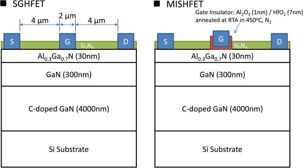
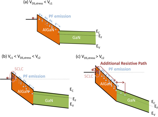
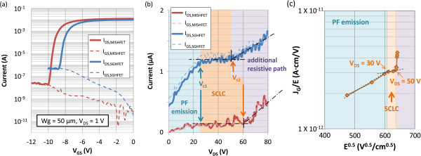
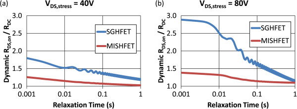
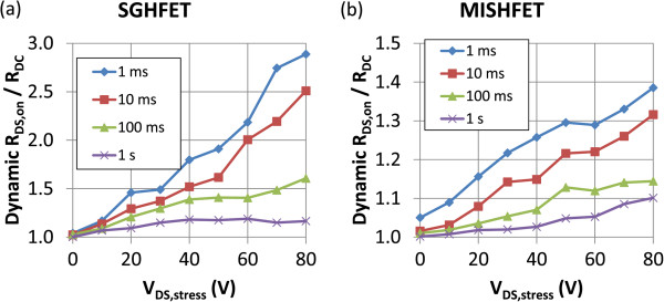
This study examined the correlation between the off-state leakage current and dynamic on-resistance (RON) transients in AlGaN/GaN heterostructure field-effect transistors (HFETs) with and without a gate insulator under various stress conditions. The RON transients in a Schottky-gate HFET (SGHFET) and metal-insulator-semiconductor HFET (MISHFET) were observed after applying various amounts of drain-source bias stress. The gate insulator in the MISHFET effectively reduced the electron injection from the gate, thereby mitigating the degradation in dynamic switching performance. However, at relaxation times exceeding 10 ms, additional detrapping occurred in both the SGHFET and MISHFET when the applied stress exceeded a critical voltage level, 50 V for the SGHFET and 60 V for MISHFET, resulting in resistive leakage current build-up and the formation of hot carriers. These high-energy carriers acted as ionized traps in the channel or buffer layers, which subsequently caused additional trapping and detrapping to occur in both HFETs during the dynamic switching test conducted.

摘要

本研究考察了在各种应力条件下,有无栅极绝缘体的AlGaN/GaN异质结构场效应晶体管(HFET)的关态漏电流与动态导通电阻(RON)瞬变之间的相关性。在施加不同量的漏源偏置应力后,观察到肖特基栅HFET(SGHFET)和金属绝缘体半导体HFET(MISHFET)中的RON瞬变。MISHFET中的栅极绝缘体有效地减少了从栅极注入的电子,从而减轻了动态开关性能的退化。然而,在弛豫时间超过10毫秒时,当施加的应力超过临界电压水平(SGHFET为50 V,MISHFET为60 V)时,SGHFET和MISHFET中都会发生额外的去俘获,导致电阻性漏电流积累和热载流子的形成。这些高能载流子在沟道或缓冲层中充当电离陷阱,随后在进行的动态开关测试期间,导致两个HFET中都发生额外的俘获和去俘获。

https://cdn.ncbi.nlm.nih.gov/pmc/blobs/f5b7/4160917/0d892cb96e78/1556-276X-9-474-5.jpg
https://cdn.ncbi.nlm.nih.gov/pmc/blobs/f5b7/4160917/d9670139e2a5/1556-276X-9-474-1.jpg
https://cdn.ncbi.nlm.nih.gov/pmc/blobs/f5b7/4160917/2c0ac3708c9f/1556-276X-9-474-2.jpg
https://cdn.ncbi.nlm.nih.gov/pmc/blobs/f5b7/4160917/991569527b95/1556-276X-9-474-3.jpg
https://cdn.ncbi.nlm.nih.gov/pmc/blobs/f5b7/4160917/a63278af768e/1556-276X-9-474-4.jpg
https://cdn.ncbi.nlm.nih.gov/pmc/blobs/f5b7/4160917/0d892cb96e78/1556-276X-9-474-5.jpg

相似文献

1
Gate leakage current induced trapping in AlGaN/GaN Schottky-gate HFETs and MISHFETs.AlGaN/GaN肖特基栅HFET和MISHFET中栅极漏电流引起的俘获
Nanoscale Res Lett. 2014 Sep 8;9(1):474. doi: 10.1186/1556-276X-9-474. eCollection 2014.
2
Proton Irradiation Effects on the Time-Dependent Dielectric Breakdown Characteristics of Normally-Off AlGaN/GaN Gate-Recessed Metal-Insulator-Semiconductor Heterostructure Field Effect Transistors.质子辐照对常关型AlGaN/GaN栅极凹陷金属-绝缘体-半导体异质结构场效应晶体管的时间相关介电击穿特性的影响
Micromachines (Basel). 2019 Oct 26;10(11):723. doi: 10.3390/mi10110723.
3
Investigation of AlGaN/GaN HFET and VO Thin Film Based Deflection Transducers Embedded in GaN Microcantilevers.基于嵌入氮化镓微悬臂梁中的氮化铝镓/氮化镓高电子迁移率晶体管和氧化钒薄膜的偏转传感器的研究。
Micromachines (Basel). 2020 Sep 20;11(9):875. doi: 10.3390/mi11090875.
4
Performance of AlGaN/GaN Nanowire Omega-Shaped-Gate Fin-Shaped Field-Effect Transistor.氮化铝镓/氮化镓纳米线Ω形栅鳍式场效应晶体管的性能
J Nanosci Nanotechnol. 2016 May;16(5):5049-52. doi: 10.1166/jnn.2016.12259.
5
Effects of Recessed-Gate Structure on AlGaN/GaN-on-SiC MIS-HEMTs with Thin AlON MIS Gate.具有薄AlON MIS栅的SiC基AlGaN/GaN凹槽栅结构MIS-HEMTs的效应
Materials (Basel). 2020 Mar 27;13(7):1538. doi: 10.3390/ma13071538.
6
Recessed-Gate GaN Metal-Insulator-Semiconductor High-Electron-Mobility Transistor Using a Dual Gate-Insulator Employing TiO₂/SiN.采用TiO₂/SiN双栅绝缘体的凹槽栅氮化镓金属绝缘体半导体高电子迁移率晶体管
J Nanosci Nanotechnol. 2020 Aug 1;20(8):4678-4683. doi: 10.1166/jnn.2020.17809.
7
Charging Effect by Fluorine-Treatment and Recess Gate for Enhancement-Mode on AlGaN/GaN High Electron Mobility Transistors.通过氟处理和凹槽栅极对AlGaN/GaN高电子迁移率晶体管增强模式的充电效应。
Nanomaterials (Basel). 2020 Oct 24;10(11):2116. doi: 10.3390/nano10112116.
8
Influence of the ratio of gate length to drain-to-source distance on the electron mobility in AlGaN/AlN/GaN heterostructure field-effect transistors.栅长与漏源距离之比对 AlGaN/AlN/GaN 异质结构场效应晶体管中电子迁移率的影响。
Nanoscale Res Lett. 2012 Aug 3;7(1):434. doi: 10.1186/1556-276X-7-434.
9
Investigation of the Gate Degradation Induced by Forward Gate Voltage Stress in p-GaN Gate High Electron Mobility Transistors.p型氮化镓栅极高电子迁移率晶体管中正向栅极电压应力引起的栅极退化研究。
Micromachines (Basel). 2023 Apr 29;14(5):977. doi: 10.3390/mi14050977.
10
AlGaN/GaN MISHEMTs with AlN gate dielectric grown by thermal ALD technique.采用热原子层沉积技术生长具有氮化铝栅介质的氮化铝镓/氮化镓金属-绝缘体-半导体高电子迁移率晶体管。
Nanoscale Res Lett. 2015 Mar 4;10:109. doi: 10.1186/s11671-015-0802-x. eCollection 2015.

引用本文的文献

1
Improvement of Dynamic On-Resistance in GaN-Based Devices with a High-Quality In Situ SiN Passivation Layer.基于高质量原位SiN钝化层的GaN基器件动态导通电阻的改善
Micromachines (Basel). 2023 Jun 10;14(6):1227. doi: 10.3390/mi14061227.
2
High Breakdown Voltage and Low Dynamic ON-Resistance AlGaN/GaN HEMT with Fluorine Ion Implantation in SiN Passivation Layer.在SiN钝化层中进行氟离子注入的具有高击穿电压和低动态导通电阻的AlGaN/GaN高电子迁移率晶体管。
Nanoscale Res Lett. 2019 Jun 4;14(1):191. doi: 10.1186/s11671-019-3025-8.
3
A High-Accuracy AlGaN/GaN Reverse Blocking CRD (RB-CRD) with Hybrid Trench Cathode.
一种具有混合沟槽阴极的高精度氮化铝镓/氮化镓反向阻断CRD(RB-CRD)。
Nanoscale Res Lett. 2019 Jan 15;14(1):23. doi: 10.1186/s11671-019-2860-y.
4
Investigation of Bulk Traps by Conductance Method in the Deep Depletion Region of the AlO/GaN MOS Device.采用电导法对AlO/GaN MOS器件深耗尽区中的体陷阱进行研究。
Nanoscale Res Lett. 2017 Dec;12(1):342. doi: 10.1186/s11671-017-2111-z. Epub 2017 May 10.
5
AlN Surface Passivation of GaN-Based High Electron Mobility Transistors by Plasma-Enhanced Atomic Layer Deposition.通过等离子体增强原子层沉积实现基于氮化镓的高电子迁移率晶体管的氮化铝表面钝化
Nanoscale Res Lett. 2017 Dec;12(1):315. doi: 10.1186/s11671-017-2082-0. Epub 2017 Apr 27.