Yin Xingtian, Battaglia Corsin, Lin Yongjing, Chen Kevin, Hettick Mark, Zheng Maxwell, Chen Cheng-Ying, Kiriya Daisuke, Javey Ali
Electrical Engineering and Computer Sciences Department, University of California , Berkeley, California 94720, United States ; Materials Sciences Division, Lawrence Berkeley National Laboratory , Berkeley, California 94720, United States ; Electronic Materials Research Laboratory, Xi'an Jiaotong University , Xi'an, 710049 Shaanxi, People's Republic of China.
Electrical Engineering and Computer Sciences Department, University of California , Berkeley, California 94720, United States ; Materials Sciences Division, Lawrence Berkeley National Laboratory , Berkeley, California 94720, United States.
ACS Photonics. 2014 Dec 17;1(12):1245-1250. doi: 10.1021/ph500153c. Epub 2014 Sep 25.
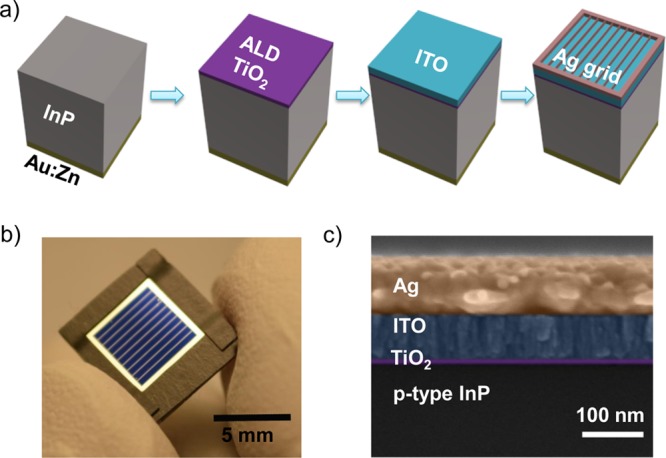
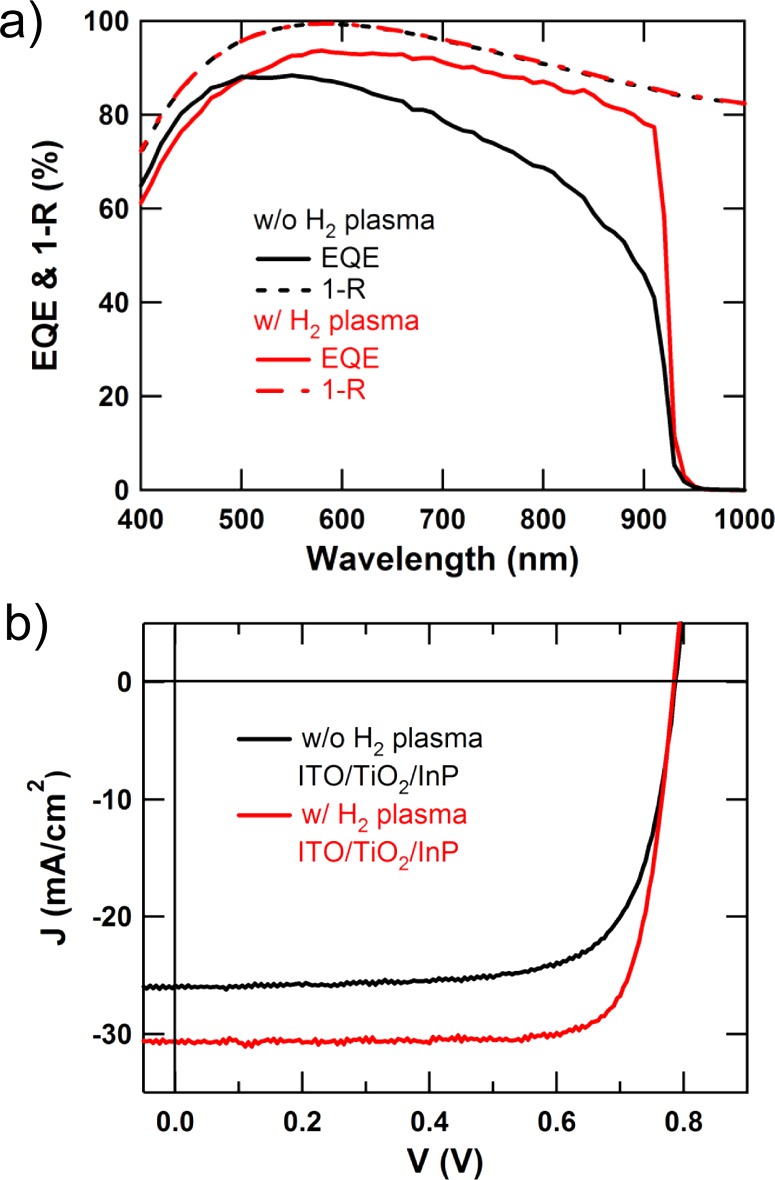
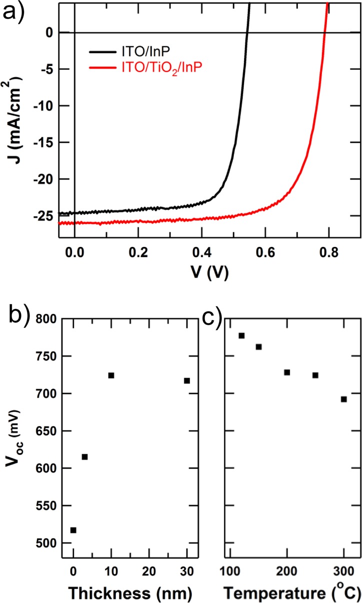
We demonstrate an InP heterojunction solar cell employing an ultrathin layer (∼10 nm) of amorphous TiO deposited at 120 °C by atomic layer deposition as the transparent electron-selective contact. The TiO film selectively extracts minority electrons from the conduction band of p-type InP while blocking the majority holes due to the large valence band offset, enabling a high maximum open-circuit voltage of 785 mV. A hydrogen plasma treatment of the InP surface drastically improves the long-wavelength response of the device, resulting in a high short-circuit current density of 30.5 mA/cm and a high power conversion efficiency of 19.2%.
我们展示了一种采用通过原子层沉积在120°C下沉积的超薄(约10nm)非晶TiO作为透明电子选择性接触的InP异质结太阳能电池。由于价带偏移大,TiO薄膜从p型InP的导带中选择性地提取少数载流子电子,同时阻挡多数载流子空穴,从而实现了785mV的高最大开路电压。对InP表面进行氢等离子体处理极大地改善了器件的长波长响应,产生了30.5mA/cm的高短路电流密度和19.2%的高功率转换效率。