Zheng Wenshan, Xie Tian, Zhou Yu, Chen Y L, Jiang Wei, Zhao Shuli, Wu Jinxiong, Jing Yumei, Wu Yue, Chen Guanchu, Guo Yunfan, Yin Jianbo, Huang Shaoyun, Xu H Q, Liu Zhongfan, Peng Hailin
Center for Nanochemistry, Beijing National Laboratory for Molecular Sciences (BNLMS), State Key Laboratory for Structural Chemistry of Unstable and Stable Species, College of Chemistry and Molecular Engineering, Peking University, Beijing 100871, P. R. China.
Department of Physics and Clarendon Laboratory, University of Oxford, Parks Road, Oxford OX1 3PU, UK.
Nat Commun. 2015 Apr 21;6:6972. doi: 10.1038/ncomms7972.
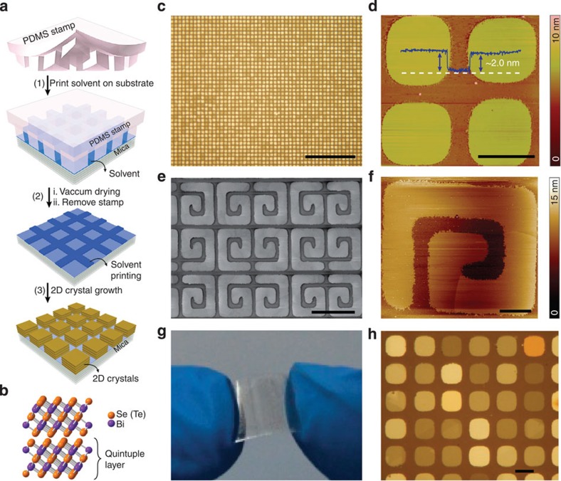
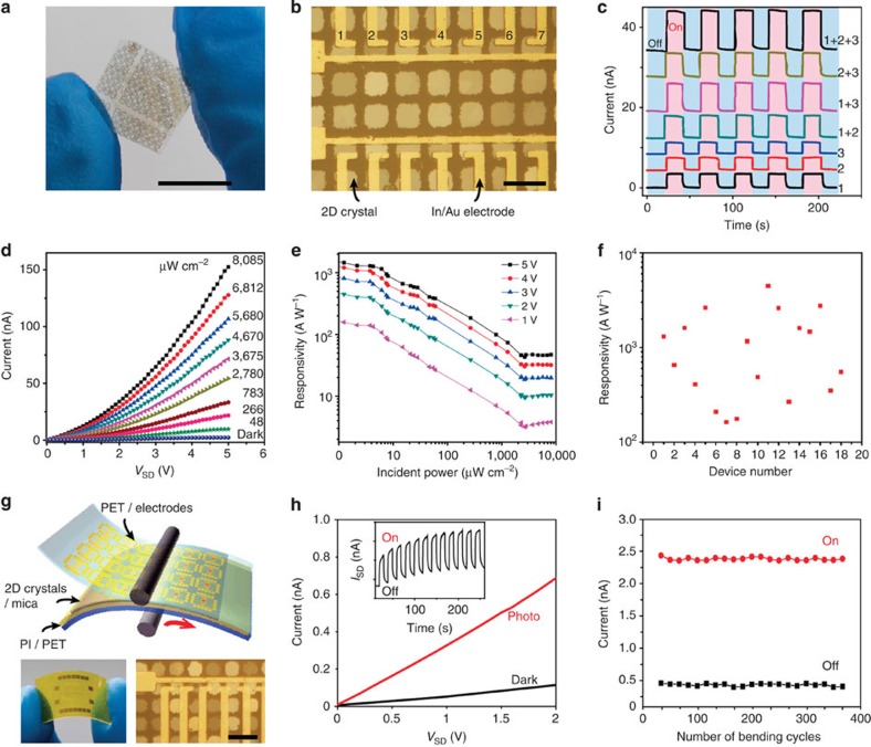
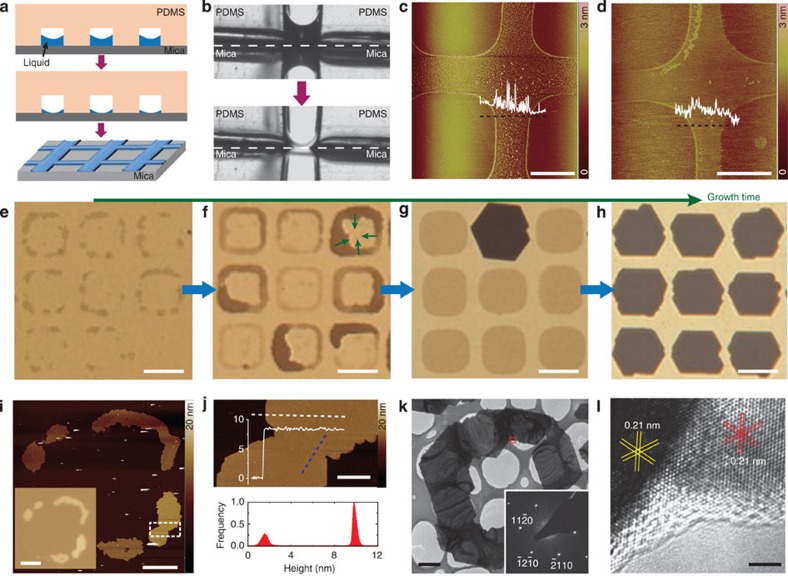
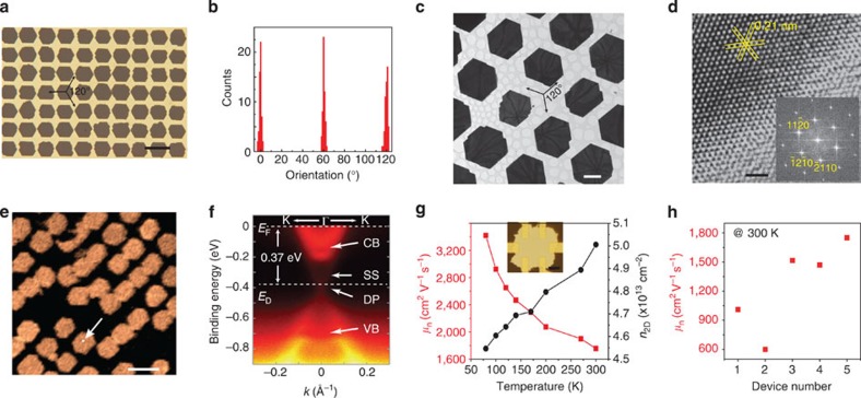
Patterning of high-quality two-dimensional chalcogenide crystals with unique planar structures and various fascinating electronic properties offers great potential for batch fabrication and integration of electronic and optoelectronic devices. However, it remains a challenge that requires accurate control of the crystallization, thickness, position, orientation and layout. Here we develop a method that combines microintaglio printing with van der Waals epitaxy to efficiently pattern various single-crystal two-dimensional chalcogenides onto transparent insulating mica substrates. Using this approach, we have patterned large-area arrays of two-dimensional single-crystal Bi2Se3 topological insulator with a record high Hall mobility of ∼1,750 cm(2) V(-1) s(-1) at room temperature. Furthermore, our patterned two-dimensional In2Se3 crystal arrays have been integrated and packaged to flexible photodetectors, yielding an ultrahigh external photoresponsivity of ∼1,650 A W(-1) at 633 nm. The facile patterning, integration and packaging of high-quality two-dimensional chalcogenide crystals hold promise for innovations of next-generation photodetector arrays, wearable electronics and integrated optoelectronic circuits.
具有独特平面结构和各种迷人电子特性的高质量二维硫族化物晶体的图案化,为电子和光电器件的批量制造和集成提供了巨大潜力。然而,这仍然是一个挑战,需要精确控制结晶、厚度、位置、取向和布局。在这里,我们开发了一种将微凹版印刷与范德华外延相结合的方法,以有效地将各种单晶二维硫族化物图案化到透明绝缘云母基板上。使用这种方法,我们已经在室温下以创纪录的约1750 cm² V⁻¹ s⁻¹的高霍尔迁移率,对二维单晶Bi2Se3拓扑绝缘体的大面积阵列进行了图案化。此外,我们图案化的二维In2Se3晶体阵列已被集成并封装到柔性光电探测器中,在633 nm处产生了约1650 A W⁻¹的超高外部光响应率。高质量二维硫族化物晶体的简便图案化、集成和封装,为下一代光电探测器阵列、可穿戴电子设备和集成光电子电路的创新带来了希望。