Xu Weijia, Yin Huaxiang, Ma Xiaolong, Hong Peizhen, Xu Miao, Meng Lingkuan
Key Laboratory of Microelectronics Devices & Integrated Technology, Institute of Microelectronics, Chinese Academy of Sciences, Beijing, 100029, China,
Nanoscale Res Lett. 2015 Dec;10(1):958. doi: 10.1186/s11671-015-0958-4. Epub 2015 Jun 2.
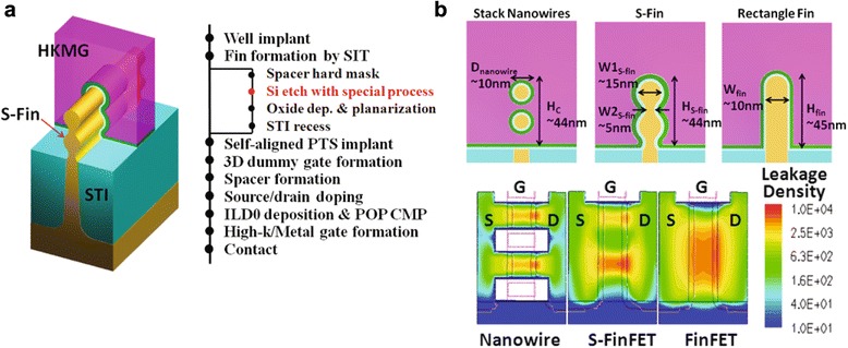
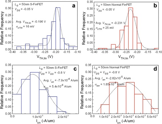
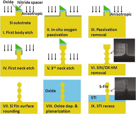
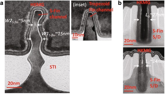
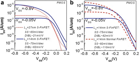
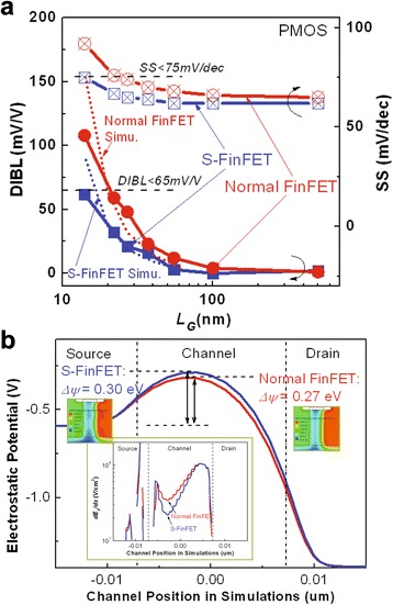
In this study, novel p-type scallop-shaped fin field-effect transistors (S-FinFETs) are fabricated using an all-last high-k/metal gate (HKMG) process on bulk-silicon (Si) substrates for the first time. In combination with the structure advantage of conventional Si nanowires, the proposed S-FinFETs provide better electrostatic integrity in the channels than normal bulk-Si FinFETs or tri-gate devices with rectangular or trapezoidal fins. It is due to formation of quasi-surrounding gate electrodes on scalloping fins by a special Si etch process. The entire integration flow of the S-FinFETs is fully compatible with the mainstream all-last HKMG FinFET process, except for a modified fin etch process. The drain-induced barrier lowering and subthreshold swing of the fabricated p-type S-FinFETs with a 14-nm physical gate length are 62 mV/V and 75 mV/dec, respectively, which are much better than those of normal FinFETs with a similar process. With an improved short-channel-effect immunity in the channels due to structure modification, the novel structure provides one of possibilities to extend the FinFET scalability to sub-10-nm nodes with little additional process cost.
在本研究中,首次在体硅(Si)衬底上采用全后段高k/金属栅(HKMG)工艺制造了新型p型扇贝形鳍式场效应晶体管(S-FinFET)。结合传统硅纳米线的结构优势,所提出的S-FinFET在沟道中比普通体硅FinFET或具有矩形或梯形鳍的三栅器件具有更好的静电完整性。这是由于通过特殊的硅蚀刻工艺在扇贝形鳍上形成了准环绕栅电极。除了改进的鳍蚀刻工艺外,S-FinFET的整个集成流程与主流的全后段HKMG FinFET工艺完全兼容。所制造的具有14nm物理栅长的p型S-FinFET的漏极诱导势垒降低和亚阈值摆幅分别为62mV/V和75mV/dec,这比采用类似工艺的普通FinFET要好得多。由于结构改进,沟道中的短沟道效应抗扰性得到提高,这种新型结构为以很少的额外工艺成本将FinFET的可扩展性扩展到10nm以下节点提供了一种可能性。