• 文献检索
  • 文档翻译
  • 深度研究
  • 学术资讯
  • Suppr Zotero 插件Zotero 插件
  • 邀请有礼
  • 套餐&价格
  • 历史记录
应用&插件
Suppr Zotero 插件Zotero 插件浏览器插件Mac 客户端Windows 客户端微信小程序
定价
高级版会员购买积分包购买API积分包
服务
文献检索文档翻译深度研究API 文档MCP 服务
关于我们
关于 Suppr公司介绍联系我们用户协议隐私条款
关注我们

Suppr 超能文献

核心技术专利:CN118964589B侵权必究
粤ICP备2023148730 号-1Suppr @ 2026

文献检索

告别复杂PubMed语法,用中文像聊天一样搜索,搜遍4000万医学文献。AI智能推荐,让科研检索更轻松。

立即免费搜索

文件翻译

保留排版,准确专业,支持PDF/Word/PPT等文件格式,支持 12+语言互译。

免费翻译文档

深度研究

AI帮你快速写综述,25分钟生成高质量综述,智能提取关键信息,辅助科研写作。

立即免费体验

二维范德瓦尔斯硒化铟晶体中的直接-间接带隙交叉。

The direct-to-indirect band gap crossover in two-dimensional van der Waals Indium Selenide crystals.

机构信息

School of Physics &Astronomy, The University of Nottingham, Nottingham, NG7 2RD, UK.

Laboratoire National des Champs Magnétiques Intenses, CNRS-UGA-UPS-INSA-EMFL, 25 rue des Martyrs, 38042 Grenoble, France.

出版信息

Sci Rep. 2016 Dec 23;6:39619. doi: 10.1038/srep39619.

DOI:10.1038/srep39619
PMID:28008964
原文链接:https://pmc.ncbi.nlm.nih.gov/articles/PMC5180233/
Abstract

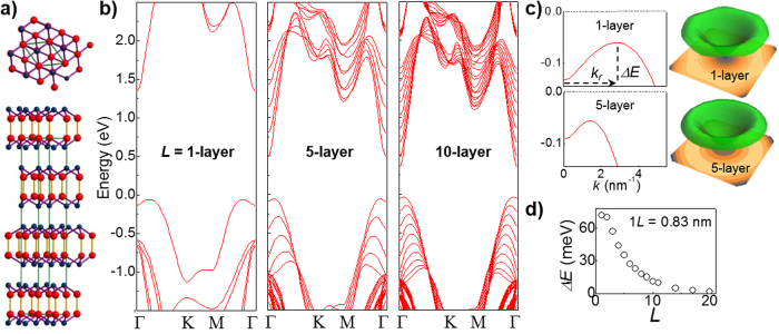
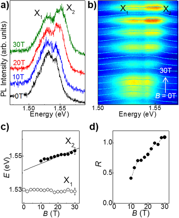
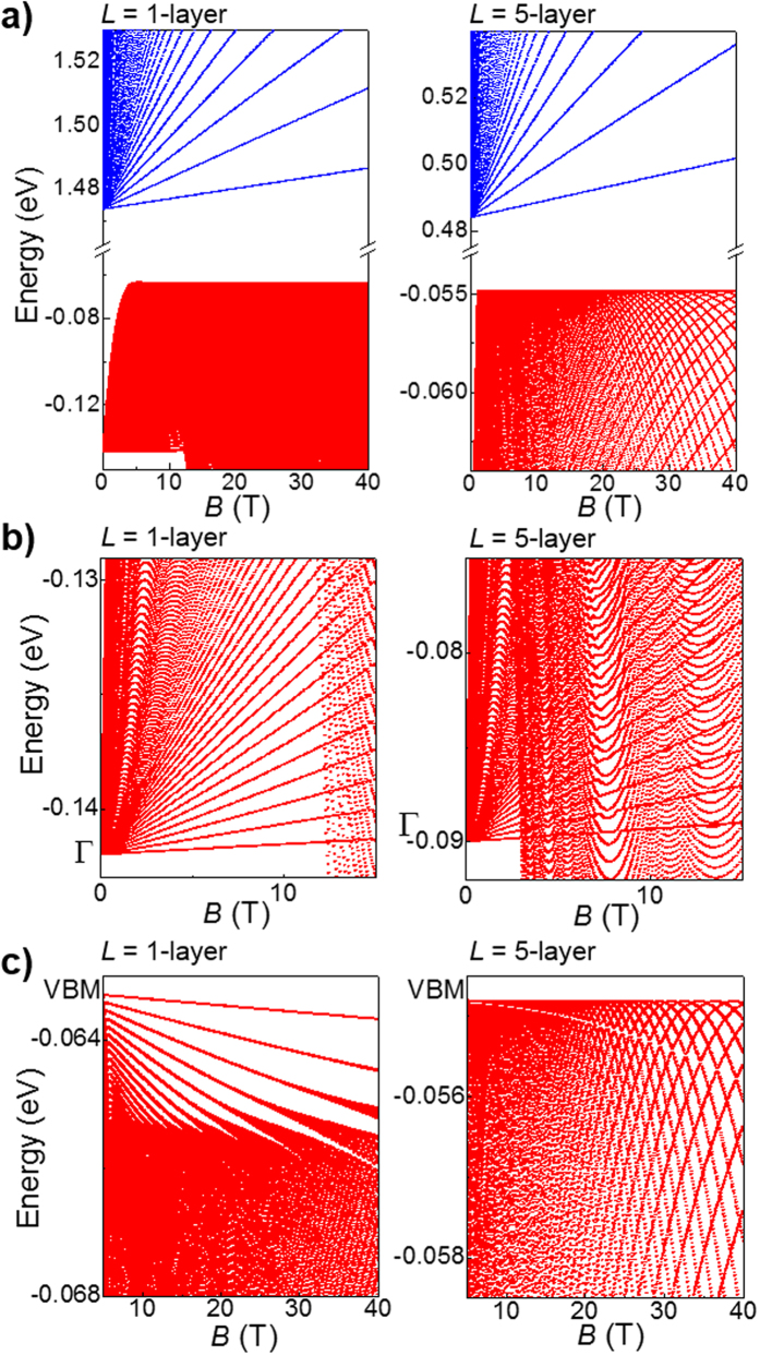
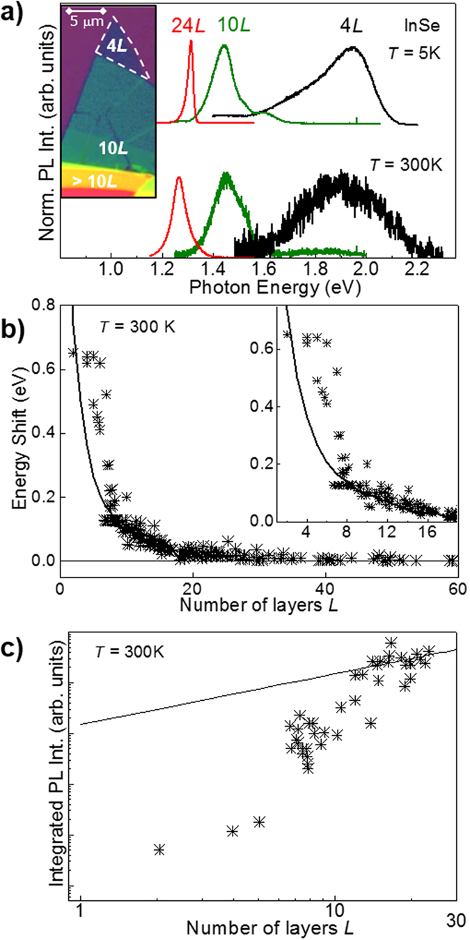
The electronic band structure of van der Waals (vdW) layered crystals has properties that depend on the composition, thickness and stacking of the component layers. Here we use density functional theory and high field magneto-optics to investigate the metal chalcogenide InSe, a recent addition to the family of vdW layered crystals, which transforms from a direct to an indirect band gap semiconductor as the number of layers is reduced. We investigate this direct-to-indirect bandgap crossover, demonstrate a highly tuneable optical response from the near infrared to the visible spectrum with decreasing layer thickness down to 2 layers, and report quantum dot-like optical emissions distributed over a wide range of energy. Our analysis also indicates that electron and exciton effective masses are weakly dependent on the layer thickness and are significantly smaller than in other vdW crystals. These properties are unprecedented within the large family of vdW crystals and demonstrate the potential of InSe for electronic and photonic technologies.

摘要

范德华(vdW)层状晶体的电子能带结构具有取决于组成、厚度和堆叠的特性。在这里,我们使用密度泛函理论和强磁场磁光来研究金属硫属化物 InSe,它是 vdW 层状晶体家族的最新成员,随着层数的减少,它从直接带隙半导体转变为间接带隙半导体。我们研究了这种直接到间接带隙的转变,证明了随着层厚度减小到 2 层,从近红外到可见光谱的高度可调谐光学响应,并报告了分布在很宽能量范围内的类似于量子点的光发射。我们的分析还表明,电子和激子有效质量对层厚度的依赖性较弱,并且比其他 vdW 晶体小得多。这些特性在 vdW 晶体的大家族中是前所未有的,展示了 InSe 在电子和光子技术中的潜力。

https://cdn.ncbi.nlm.nih.gov/pmc/blobs/76b7/5180233/446e45bc4b65/srep39619-f6.jpg
https://cdn.ncbi.nlm.nih.gov/pmc/blobs/76b7/5180233/2e8adad396b2/srep39619-f1.jpg
https://cdn.ncbi.nlm.nih.gov/pmc/blobs/76b7/5180233/1efaf8c05601/srep39619-f2.jpg
https://cdn.ncbi.nlm.nih.gov/pmc/blobs/76b7/5180233/78e25f8b063d/srep39619-f3.jpg
https://cdn.ncbi.nlm.nih.gov/pmc/blobs/76b7/5180233/8737a27942fb/srep39619-f4.jpg
https://cdn.ncbi.nlm.nih.gov/pmc/blobs/76b7/5180233/4080b533d613/srep39619-f5.jpg
https://cdn.ncbi.nlm.nih.gov/pmc/blobs/76b7/5180233/446e45bc4b65/srep39619-f6.jpg

相似文献

1
The direct-to-indirect band gap crossover in two-dimensional van der Waals Indium Selenide crystals.二维范德瓦尔斯硒化铟晶体中的直接-间接带隙交叉。
Sci Rep. 2016 Dec 23;6:39619. doi: 10.1038/srep39619.
2
Two-Dimensional Covalent Crystals by Chemical Conversion of Thin van der Waals Materials.通过范德华薄材料的化学转化制备二维共价晶体
Nano Lett. 2019 Sep 11;19(9):6475-6481. doi: 10.1021/acs.nanolett.9b02700. Epub 2019 Aug 26.
3
Photoacoustic and modulated reflectance studies of indirect and direct band gap in van der Waals crystals.范德华晶体中间接和直接带隙的光声与调制反射研究。
Sci Rep. 2017 Nov 13;7(1):15365. doi: 10.1038/s41598-017-15763-1.
4
Indirect to Direct Gap Crossover in Two-Dimensional InSe Revealed by Angle-Resolved Photoemission Spectroscopy.角分辨光电子能谱揭示二维InSe中的间接到直接能隙交叉
ACS Nano. 2019 Feb 26;13(2):2136-2142. doi: 10.1021/acsnano.8b08726. Epub 2019 Jan 28.
5
Electronic and Transport Properties of InSe/PtTe van der Waals Heterostructure.InSe/PtTe范德华异质结构的电学和输运性质
Nano Lett. 2024 Jul 10;24(27):8402-8409. doi: 10.1021/acs.nanolett.4c02067. Epub 2024 Jun 27.
6
Tuning the bandgap of exfoliated InSe nanosheets by quantum confinement.通过量子限域来调节剥离的 InSe 纳米片的带隙。
Adv Mater. 2013 Oct 25;25(40):5714-8. doi: 10.1002/adma.201302616. Epub 2013 Aug 21.
7
Gate-Defined Quantum Confinement in InSe-Based van der Waals Heterostructures.基于 InSe 的范德瓦尔斯异质结构中的栅极定义量子限制。
Nano Lett. 2018 Jun 13;18(6):3950-3955. doi: 10.1021/acs.nanolett.8b01376. Epub 2018 May 21.
8
Silicene and germanene on InSe substrates: structures and tunable electronic properties.硒铟铜衬底上的硅烯和锗烯:结构与可调电子特性
Phys Chem Chem Phys. 2018 Apr 25;20(16):11369-11377. doi: 10.1039/c8cp00610e.
9
Tunable electronic properties of an Sb/InSe van der Waals heterostructure by electric field effects.通过电场效应实现 Sb/InSe 范德华异质结构的可调谐电子性质。
Phys Chem Chem Phys. 2019 Mar 6;21(10):5627-5633. doi: 10.1039/c8cp07407k.
10
High broad-band photoresponsivity of mechanically formed InSe-graphene van der Waals heterostructures.机械形成的InSe-石墨烯范德华异质结构的高宽带光响应性。
Adv Mater. 2015 Jul 1;27(25):3760-6. doi: 10.1002/adma.201500889. Epub 2015 May 15.

引用本文的文献

1
Brightening dark excitons and trions in systems with a Mexican-hat energy dispersion: example of InSe.在具有墨西哥帽能量色散的系统中增强暗激子和三重态激子:以硒化铟为例。
NPJ 2D Mater Appl. 2025;9(1):63. doi: 10.1038/s41699-025-00570-4. Epub 2025 Jul 21.
2
Low-dimensional solid-state single-photon emitters.低维固态单光子发射器
Nanophotonics. 2025 Jan 8;14(11):1687-1713. doi: 10.1515/nanoph-2024-0569. eCollection 2025 Jun.
3
Giant Light Emission Enhancement in Strain-Engineered InSe/MS (M = Mo or W) van der Waals Heterostructures.

本文引用的文献

1
High electron mobility, quantum Hall effect and anomalous optical response in atomically thin InSe.原子层厚 InSe 中的高电子迁移率、量子霍尔效应和反常光响应。
Nat Nanotechnol. 2017 Mar;12(3):223-227. doi: 10.1038/nnano.2016.242. Epub 2016 Nov 21.
2
Nanotexturing To Enhance Photoluminescent Response of Atomically Thin Indium Selenide with Highly Tunable Band Gap.纳米织构化提高原子层厚硒化铟的光致发光响应,其带隙可调谐性高。
Nano Lett. 2016 May 11;16(5):3221-9. doi: 10.1021/acs.nanolett.6b00689. Epub 2016 Apr 19.
3
The influence of chemical reactivity of surface defects on ambient-stable InSe-based nanodevices.
应变工程InSe/MS(M = Mo或W)范德华异质结构中的巨光发射增强
Nano Lett. 2025 Mar 5;25(9):3375-3382. doi: 10.1021/acs.nanolett.4c04252. Epub 2025 Feb 5.
4
Spin polarization detection via chirality-induced tunnelling currents in indium selenide.通过硒化铟中手性诱导隧穿电流进行自旋极化检测
Nat Mater. 2025 Feb;24(2):212-218. doi: 10.1038/s41563-024-02067-9. Epub 2025 Jan 8.
5
Probing the Electronic and Opto-Electronic Properties of Multilayer MoS Field-Effect Transistors at Low Temperatures.低温下多层MoS场效应晶体管的电学和光电特性探究
Nanomaterials (Basel). 2023 Aug 14;13(16):2333. doi: 10.3390/nano13162333.
6
Recent Advances for the Synthesis and Applications of 2-Dimensional Ternary Layered Materials.二维三元层状材料的合成与应用研究进展
Research (Wash D C). 2023;6:0040. doi: 10.34133/research.0040. Epub 2023 Jan 30.
7
Subnanometer-Wide Indium Selenide Nanoribbons.亚纳米宽的硒化铟纳米带。
ACS Nano. 2023 Mar 28;17(6):6062-6072. doi: 10.1021/acsnano.3c00670. Epub 2023 Mar 14.
8
Influence of Ce, Nd, Eu and Tm Dopants on the Properties of InSe Monolayer: A First-Principles Study.铈、钕、铕和铥掺杂剂对InSe单层性质的影响:第一性原理研究
Nanomaterials (Basel). 2021 Oct 14;11(10):2707. doi: 10.3390/nano11102707.
9
Single-molecule photocatalytic dynamics at individual defects in two-dimensional layered materials.二维层状材料中单个缺陷处的单分子光催化动力学
Sci Adv. 2021 Oct;7(40):eabj4452. doi: 10.1126/sciadv.abj4452. Epub 2021 Oct 1.
10
Resonance and antiresonance in Raman scattering in GaSe and InSe crystals.GaSe和InSe晶体中拉曼散射的共振与反共振
Sci Rep. 2021 Jan 13;11(1):924. doi: 10.1038/s41598-020-79411-x.
表面缺陷的化学反应性对环境稳定的基于 InSe 的纳米器件的影响。
Nanoscale. 2016 Apr 28;8(16):8474-9. doi: 10.1039/c6nr01262k. Epub 2016 Apr 6.
4
Spin splitting in 2D monochalcogenide semiconductors.二维单硫属化物半导体中的自旋分裂
Sci Rep. 2015 Nov 24;5:17044. doi: 10.1038/srep17044.
5
Two-Dimensional Indium Selenides Compounds: An Ab Initio Study.二维铟硒化合物:一项从头算研究。
J Phys Chem Lett. 2015 Aug 6;6(15):3098-103. doi: 10.1021/acs.jpclett.5b01356. Epub 2015 Jul 24.
6
Tunable Magnetism and Half-Metallicity in Hole-Doped Monolayer GaSe.空穴掺杂单层 GaSe 中的可调磁性和半金属性。
Phys Rev Lett. 2015 Jun 12;114(23):236602. doi: 10.1103/PhysRevLett.114.236602. Epub 2015 Jun 8.
7
High broad-band photoresponsivity of mechanically formed InSe-graphene van der Waals heterostructures.机械形成的InSe-石墨烯范德华异质结构的高宽带光响应性。
Adv Mater. 2015 Jul 1;27(25):3760-6. doi: 10.1002/adma.201500889. Epub 2015 May 15.
8
Single photon emitters in exfoliated WSe2 structures.单层二硒化钨结构中的单光子发射器。
Nat Nanotechnol. 2015 Jun;10(6):503-6. doi: 10.1038/nnano.2015.67. Epub 2015 May 4.
9
Single quantum emitters in monolayer semiconductors.单层半导体中的单量子发射器。
Nat Nanotechnol. 2015 Jun;10(6):497-502. doi: 10.1038/nnano.2015.75. Epub 2015 May 4.
10
Optically active quantum dots in monolayer WSe2.单层 WSe2 中的手性量子点。
Nat Nanotechnol. 2015 Jun;10(6):491-6. doi: 10.1038/nnano.2015.60. Epub 2015 May 4.