Photonics Devices and Systems Group, SUTD-MIT International Design Center, Singapore University of Technology and Design, 8 Somapah Road, Singapore 487372, Singapore.
Data Storage Institute, Agency for Science, Technology and Research (A*STAR), 2 Fusionopolis Way #08-01, Innovis 138634, Singapore.
Nat Commun. 2017 Jan 4;8:13878. doi: 10.1038/ncomms13878.
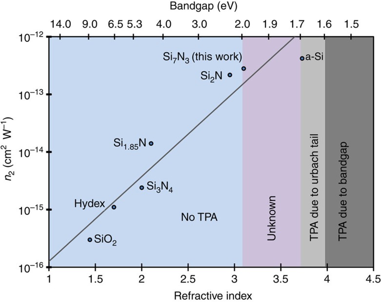
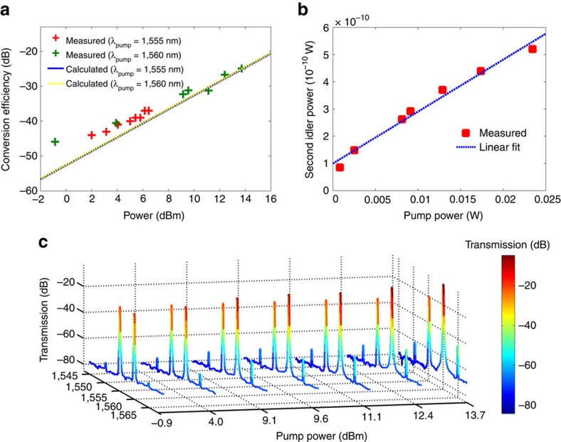
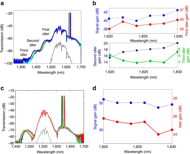
CMOS platforms operating at the telecommunications wavelength either reside within the highly dissipative two-photon regime in silicon-based optical devices, or possess small nonlinearities. Bandgap engineering of non-stoichiometric silicon nitride using state-of-the-art fabrication techniques has led to our development of USRN (ultra-silicon-rich nitride) in the form of SiN, that possesses a high Kerr nonlinearity (2.8 × 10 cm W), an order of magnitude larger than that in stoichiometric silicon nitride. Here we experimentally demonstrate high-gain optical parametric amplification using USRN, which is compositionally tailored such that the 1,550 nm wavelength resides above the two-photon absorption edge, while still possessing large nonlinearities. Optical parametric gain of 42.5 dB, as well as cascaded four-wave mixing with gain down to the third idler is observed and attributed to the high photon efficiency achieved through operating above the two-photon absorption edge, representing one of the largest optical parametric gains to date on a CMOS platform.
CMOS 平台在电信波长下运行,要么位于基于硅的光器件中的高耗散双光子区,要么具有较小的非线性。使用最先进的制造技术对非化学计量氮化硅进行能带工程设计,导致我们以 SiN 的形式开发了 USRN(超富硅氮化物),其具有高克尔非线性(2.8×10⁻¹⁰cm2/W),比化学计量氮化硅大一个数量级。在这里,我们实验演示了使用 USRN 的高增益光参量放大,其组成经过精心设计,使得 1550nm 波长位于双光子吸收边缘之上,同时仍具有较大的非线性。观察到 42.5dB 的光参量增益,以及增益降低到第三个闲频光的级联四波混频,并归因于通过在双光子吸收边缘以上操作实现的高光子效率,这是迄今为止在 CMOS 平台上获得的最大光参量增益之一。