• 文献检索
  • 文档翻译
  • 深度研究
  • 学术资讯
  • Suppr Zotero 插件Zotero 插件
  • 邀请有礼
  • 套餐&价格
  • 历史记录
应用&插件
Suppr Zotero 插件Zotero 插件浏览器插件Mac 客户端Windows 客户端微信小程序
定价
高级版会员购买积分包购买API积分包
服务
文献检索文档翻译深度研究API 文档MCP 服务
关于我们
关于 Suppr公司介绍联系我们用户协议隐私条款
关注我们

Suppr 超能文献

核心技术专利:CN118964589B侵权必究
粤ICP备2023148730 号-1Suppr @ 2026

文献检索

告别复杂PubMed语法,用中文像聊天一样搜索,搜遍4000万医学文献。AI智能推荐,让科研检索更轻松。

立即免费搜索

文件翻译

保留排版,准确专业,支持PDF/Word/PPT等文件格式,支持 12+语言互译。

免费翻译文档

深度研究

AI帮你快速写综述,25分钟生成高质量综述,智能提取关键信息,辅助科研写作。

立即免费体验

二维半导体的模型介电函数,包括衬底屏蔽。

Model dielectric function for 2D semiconductors including substrate screening.

机构信息

Laboratoire des Solides Irradiés, Ecole polytechnique, CNRS, CEA, Université Paris-Saclay, 91128 Palaiseau, France.

European Theoretical Spectroscopy Facility, 91128 Palaiseau, France.

出版信息

Sci Rep. 2017 Jan 24;7:39844. doi: 10.1038/srep39844.

DOI:10.1038/srep39844
PMID:28117326
原文链接:https://pmc.ncbi.nlm.nih.gov/articles/PMC5259763/
Abstract

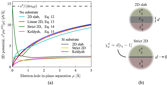
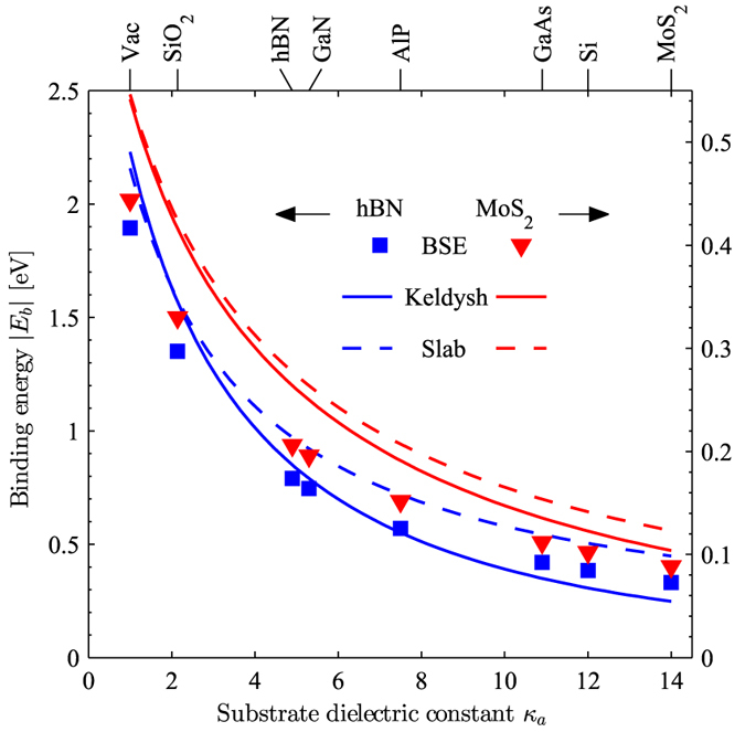
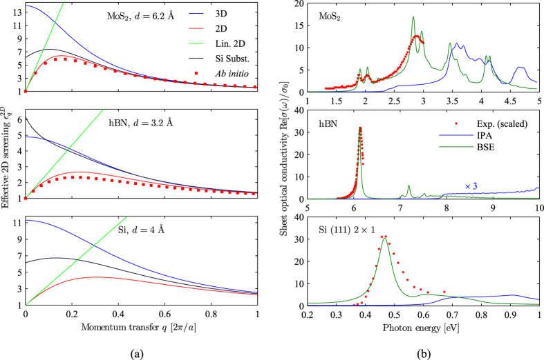
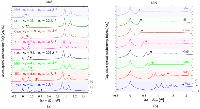
Dielectric screening of excitons in 2D semiconductors is known to be a highly non-local effect, which in reciprocal space translates to a strong dependence on momentum transfer q. We present an analytical model dielectric function, including the full non-linear q-dependency, which may be used as an alternative to more numerically taxing ab initio screening functions. By verifying the good agreement between excitonic optical properties calculated using our model dielectric function, and those derived from ab initio methods, we demonstrate the versatility of this approach. Our test systems include: Monolayer hBN, monolayer MoS, and the surface exciton of a 2 × 1 reconstructed Si(111) surface. Additionally, using our model, we easily take substrate screening effects into account. Hence, we include also a systematic study of the effects of substrate media on the excitonic optical properties of MoS and hBN.

摘要

二维半导体中的激子介电屏蔽是一种高度非局域的效应,在倒空间中表现为对动量转移 q 的强烈依赖。我们提出了一种解析介电函数模型,包括完整的非线性 q 依赖性,可作为更具数值挑战性的从头算屏蔽函数的替代方法。通过验证使用我们的介电函数模型计算的激子光学性质与从头算方法得出的结果之间的良好一致性,我们证明了这种方法的多功能性。我们的测试系统包括:单层 hBN、单层 MoS2 和 2×1 重构 Si(111)表面的表面激子。此外,我们使用模型可以轻松考虑衬底屏蔽效应。因此,我们还系统地研究了衬底介质对 MoS2 和 hBN 的激子光学性质的影响。

https://cdn.ncbi.nlm.nih.gov/pmc/blobs/dc73/5259763/a778416217d4/srep39844-f4.jpg
https://cdn.ncbi.nlm.nih.gov/pmc/blobs/dc73/5259763/357965ec0863/srep39844-f1.jpg
https://cdn.ncbi.nlm.nih.gov/pmc/blobs/dc73/5259763/67e7c5464dd6/srep39844-f2.jpg
https://cdn.ncbi.nlm.nih.gov/pmc/blobs/dc73/5259763/ea1ed0c88023/srep39844-f3.jpg
https://cdn.ncbi.nlm.nih.gov/pmc/blobs/dc73/5259763/a778416217d4/srep39844-f4.jpg

相似文献

1
Model dielectric function for 2D semiconductors including substrate screening.二维半导体的模型介电函数,包括衬底屏蔽。
Sci Rep. 2017 Jan 24;7:39844. doi: 10.1038/srep39844.
2
Dielectric environment and/or random disorder effects on free, charged and localized excitonic states in monolayer WS.单层WS中自由、带电和局域激子态的介电环境和/或随机无序效应。
J Phys Condens Matter. 2017 Nov 1;29(43):435305. doi: 10.1088/1361-648X/aa85f3.
3
Controlled dynamic screening of excitonic complexes in 2D semiconductors.二维半导体中激子复合物的控制动态筛选。
Sci Rep. 2018 Jan 15;8(1):768. doi: 10.1038/s41598-017-18803-y.
4
Phonon Screening of Excitons in Semiconductors: Halide Perovskites and Beyond.半导体中激子的声子屏蔽:卤化物钙钛矿及其他材料
Phys Rev Lett. 2021 Aug 6;127(6):067401. doi: 10.1103/PhysRevLett.127.067401.
5
Electronic structure and optical signatures of semiconducting transition metal dichalcogenide nanosheets.半导体过渡金属二卤化物纳米片的电子结构和光学特征。
Acc Chem Res. 2015 Jan 20;48(1):91-9. doi: 10.1021/ar500303m. Epub 2014 Dec 17.
6
Time-Dependent Screening Explains the Ultrafast Excitonic Signal Rise in 2D Semiconductors.时间相关筛选解释了二维半导体中超快激子信号的上升。
ACS Nano. 2021 Jan 26;15(1):1179-1185. doi: 10.1021/acsnano.0c08173. Epub 2020 Dec 31.
7
Substrate effect on excitonic shift and radiative lifetime of two-dimensional materials.二维材料中激子跃迁和辐射寿命的衬底效应
J Phys Condens Matter. 2021 May 11;33(23). doi: 10.1088/1361-648X/abeacf.
8
A method to restore the intrinsic dielectric functions of 2D materials in periodic calculations.一种在周期性计算中恢复二维材料本征介电函数的方法。
Nanoscale. 2021 Oct 21;13(40):17057-17067. doi: 10.1039/d1nr04896a.
9
Dynamical Excitonic Effects in Doped Two-Dimensional Semiconductors.掺杂二维半导体中的动力学激子效应。
Nano Lett. 2016 Sep 14;16(9):5568-73. doi: 10.1021/acs.nanolett.6b02118. Epub 2016 Aug 4.
10
Exciton-dominated Dielectric Function of Atomically Thin MoS2 Films.原子级薄MoS₂薄膜的激子主导介电函数
Sci Rep. 2015 Nov 24;5:16996. doi: 10.1038/srep16996.

引用本文的文献

1
Roadmap for Photonics with 2D Materials.二维材料光子学路线图
ACS Photonics. 2025 Jul 24;12(8):3961-4095. doi: 10.1021/acsphotonics.5c00353. eCollection 2025 Aug 20.
2
Breakdown of the Static Dielectric Screening Approximation of Coulomb Interactions in Atomically Thin Semiconductors.原子级薄半导体中库仑相互作用的静态介电屏蔽近似的失效
ACS Nano. 2025 Feb 4;19(4):4269-4278. doi: 10.1021/acsnano.4c11563. Epub 2025 Jan 21.
3
The Key Role of Non-Local Screening in the Environment-Insensitive Exciton Fine Structures of Transition-Metal Dichalcogenide Monolayers.

本文引用的文献

1
Exciton Band Structure in Two-Dimensional Materials.二维材料中的激子能带结构
Phys Rev Lett. 2016 Feb 12;116(6):066803. doi: 10.1103/PhysRevLett.116.066803. Epub 2016 Feb 10.
2
Solution-Processed Dielectrics Based on Thickness-Sorted Two-Dimensional Hexagonal Boron Nitride Nanosheets.基于厚度分级二维六方氮化硼纳米片的溶液处理电介质。
Nano Lett. 2015 Oct 14;15(10):7029-36. doi: 10.1021/acs.nanolett.5b03075. Epub 2015 Sep 10.
3
Dielectric Genome of van der Waals Heterostructures.范德瓦尔斯异质结构的介电基因组
非局域筛选在过渡金属二硫属化物单层对环境不敏感的激子精细结构中的关键作用。
Nanomaterials (Basel). 2023 May 26;13(11):1739. doi: 10.3390/nano13111739.
4
Magnon Straintronics in the 2D van der Waals Ferromagnet CrSBr from First-Principles.基于第一性原理研究二维范德华铁磁体CrSBr中的马格农自旋电子学
Nano Lett. 2022 Nov 9;22(21):8771-8778. doi: 10.1021/acs.nanolett.2c02863. Epub 2022 Sep 26.
5
Machine learning dielectric screening for the simulation of excited state properties of molecules and materials.用于分子和材料激发态性质模拟的机器学习介电屏蔽
Chem Sci. 2021 Mar 2;12(13):4970-4980. doi: 10.1039/d1sc00503k.
6
Interlayer excitons in van der Waals heterostructures: Binding energy, Stark shift, and field-induced dissociation.范德华异质结构中的层间激子:结合能、斯塔克位移和场致离解
Sci Rep. 2020 Mar 26;10(1):5537. doi: 10.1038/s41598-020-62431-y.
7
Exciton fission in monolayer transition metal dichalcogenide semiconductors.单层过渡金属二卤族化合物半导体中的激子分裂。
Nat Commun. 2017 Oct 27;8(1):1166. doi: 10.1038/s41467-017-01298-6.
8
Coulomb engineering of the bandgap and excitons in two-dimensional materials.二维材料中带隙和激子的库仑工程。
Nat Commun. 2017 May 4;8:15251. doi: 10.1038/ncomms15251.
Nano Lett. 2015 Jul 8;15(7):4616-21. doi: 10.1021/acs.nanolett.5b01251. Epub 2015 Jun 12.
4
Optical spectrum of MoS2: many-body effects and diversity of exciton states.MoS2 的光学光谱:多体效应和激子态的多样性。
Phys Rev Lett. 2013 Nov 22;111(21):216805. doi: 10.1103/PhysRevLett.111.216805. Epub 2013 Nov 20.
5
Stacking order dependent second harmonic generation and topological defects in h-BN bilayers.堆叠顺序相关的双层 h-BN 中的二次谐波产生和拓扑缺陷。
Nano Lett. 2013;13(11):5660-5. doi: 10.1021/nl403328s. Epub 2013 Oct 16.
6
Excitons in boron nitride nanotubes: dimensionality effects.氮化硼纳米管中的激子:维度效应。
Phys Rev Lett. 2006 Mar 31;96(12):126104. doi: 10.1103/PhysRevLett.96.126104. Epub 2006 Mar 30.
7
Quasi-one-dimensional excitons and the optical properties of Si(111)2 x 1.准一维激子与Si(111)2×1的光学性质
Phys Rev Lett. 1991 Dec 30;67(27):3816-3819. doi: 10.1103/PhysRevLett.67.3816.
8
Many-body calculation of the surface-state energies for Si(111)2 x 1.硅(111)2×1表面态能量的多体计算
Phys Rev Lett. 1991 Jan 28;66(4):500-503. doi: 10.1103/PhysRevLett.66.500.
9
Electron-phonon interaction in optical absorption at the Si(111)2 x 1 surface.硅(111)2×1表面光吸收中的电子 - 声子相互作用
Phys Rev Lett. 1986 Jun 2;56(22):2411-2414. doi: 10.1103/PhysRevLett.56.2411.
10
Model dielectric function for semiconductors.半导体的模型介电函数。
Phys Rev B Condens Matter. 1993 Apr 15;47(15):9892-9895. doi: 10.1103/physrevb.47.9892.